N80C151SA 查看數據表(PDF) - Intel
零件编号
产品描述 (功能)
生产厂家
N80C151SA Datasheet PDF : 33 Pages
| |||
8XC151SA SB HIGH-PERFORMANCE CHMOS MICROCONTROLLER
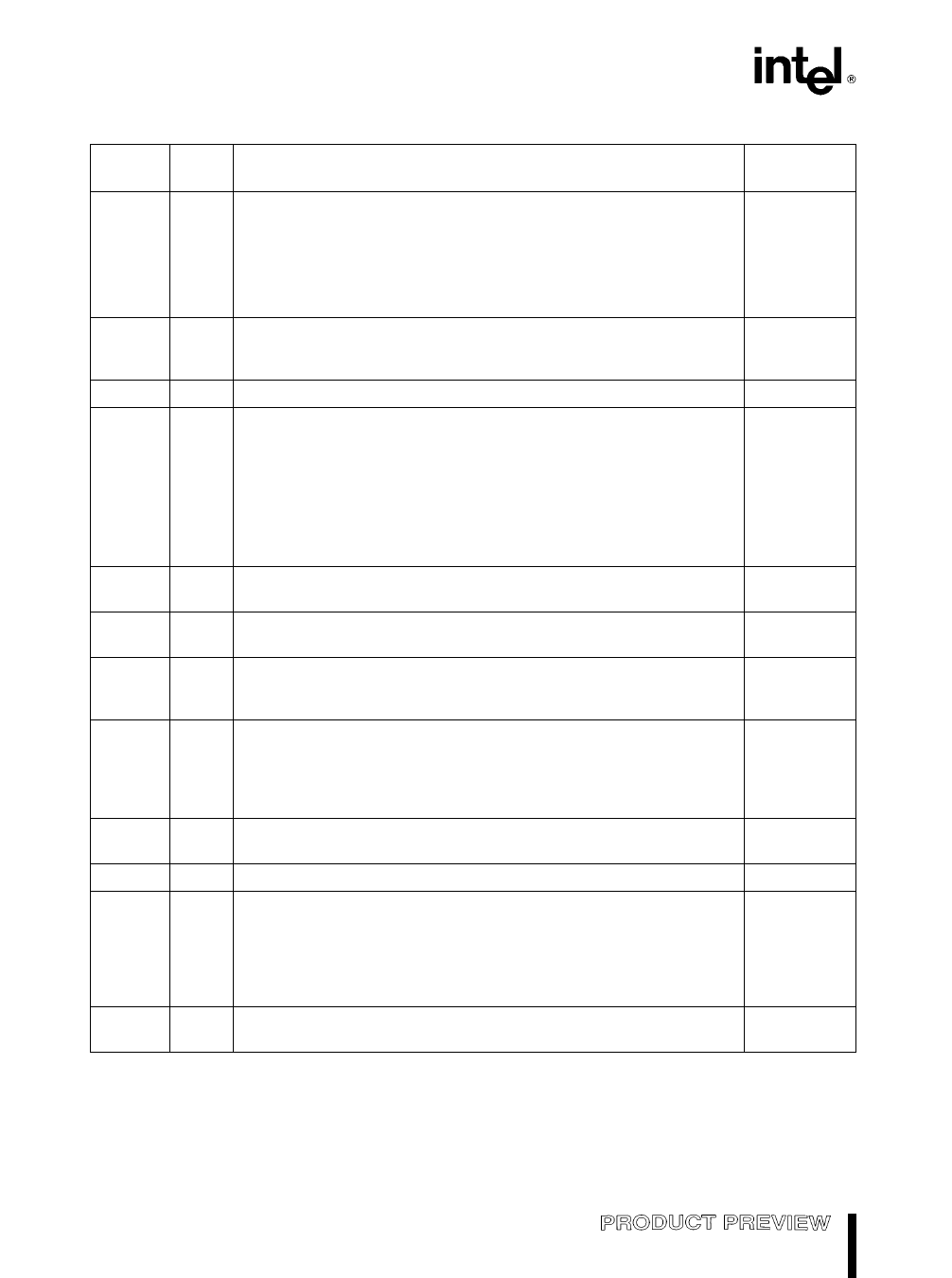
Table 7 Signal Descriptions (Continued)
Signal
Name
Type
Description
Multiplexed
With
P3 0
P3 1
P3 3 2
P3 5 4
P3 6
P3 7
I O Port 3 This is an 8-bit bidirectional I O port with internal pullups
RXD
TXD
INT1 0
T1 0
WR
RD
PSEN
O Program Store Enable Read signal output This output is asserted
for a memory address range that depends on bits RD0 and RD1 in
configuration byte UCONFIG0
RD
O Read Read signal output to external data memory
P3 7
RST
I
Reset Reset input to the chip Holding this pin high for 64 oscillator
periods while the oscillator is running resets the device The port pins
are driven to their reset conditions when a voltage greater than VIH1 is
applied whether or not the oscillator is running This pin has an
internal pulldown resistor which allows the device to be reset by
connecting a capacitor between this pin and VCC
Asserting RST when the chip is in idle mode or powerdown mode
returns the chip to normal operation
RXD
I O Receive Serial Data RXD sends and receives data in serial I O
mode 0 and receives data in serial I O modes 1 2 and 3
P3 0
T1 0
I
Timer 1 0 External Clock Inputs When timer 1 0 operates as a
counter a falling edge on the T1 0 pin increments the count
P3 5 4
T2
I O Timer 2 Clock Input Output For the timer 2 capture mode this
signal is the external clock input For the clock-out mode it is the
timer 2 clock output
P1 0
T2EX
I
Timer 2 External Input In timer 2 capture mode a falling edge
initiates a capture of the timer 2 registers In auto-reload mode a
falling edge causes the timer 2 registers to be reloaded In the up-
down counter mode this signal determines the count direction
1 e up 0 e down
P1 1
TXD
O Transmit Serial Data TXD outputs the shift clock in serial I O mode
P3 1
0 and transmits serial data in serial I O modes 1 2 and 3
VCC
VCC2
PWR
PWR
Supply Voltage Connect this pin to the a5V supply voltage
Secondary Supply Voltage 2 This supply voltage connection is
provided to reduce power supply noise Connection of this pin to the
a5V supply voltage is recommended However when using the
8XC151SA SB as a pin-for-pin replacement for the 8XC51FX VSS2
can be unconnected without loss of compatibility (Not available on
DIP)
VPP
I
Programming Supply Voltage The programming supply voltage is
EA
applied to this pin for programming the on-chip OTPROM
The descriptions of A15 8 P2 7 0 and AD7 0 P0 7 0 are for the nonpage-mode chip configuration (compatible with
44-lead PLCC and 40-pin DIP MCS 51 microcontrollers) If the chip is configured for page-mode operation port 0 carries
the lower address bits (A7 0) and port 2 carries the upper address bits (A15 8) and the data (D7 0)
10
Share Link: 