NT2H0301F0DTL,125 查看數據表(PDF) - NXP Semiconductors.
零件编号
产品描述 (功能)
生产厂家
NT2H0301F0DTL,125
NXP Semiconductors.

NT2H0301F0DTL,125 Datasheet PDF : 31 Pages
| |||
NXP Semiconductors
NTAG203F
NFC Forum compliant IC with user memory and field detection
7.5.2 Lock bytes
Lock bytes enable the user to lock parts of the complete memory area for writing. A Read
from user memory area cannot be restricted via lock bytes functionality.
The lock bytes functionality is enabled with a WRITE command (see Section 7.9.7
“WRITE”) or COMPATIBILITY WRITE command (see Section 7.9.8 “COMPATIBILITY
WRITE”), where 2 out of 4 bytes transmitted are used for setting the lock bytes. Two
corresponding bytes - either bytes 2 and 3 for page 02h or bytes 0 and 1 for page 28h -
and the actual content of the lock bytes are bit-wise “OR-ed”. The result of OR operation
becomes the new content of the lock bytes. Two unused bytes do not have to be
considered. Although included in the COMPATIBILITY WRITE or WRITE command, they
are ignored when programming the memory.
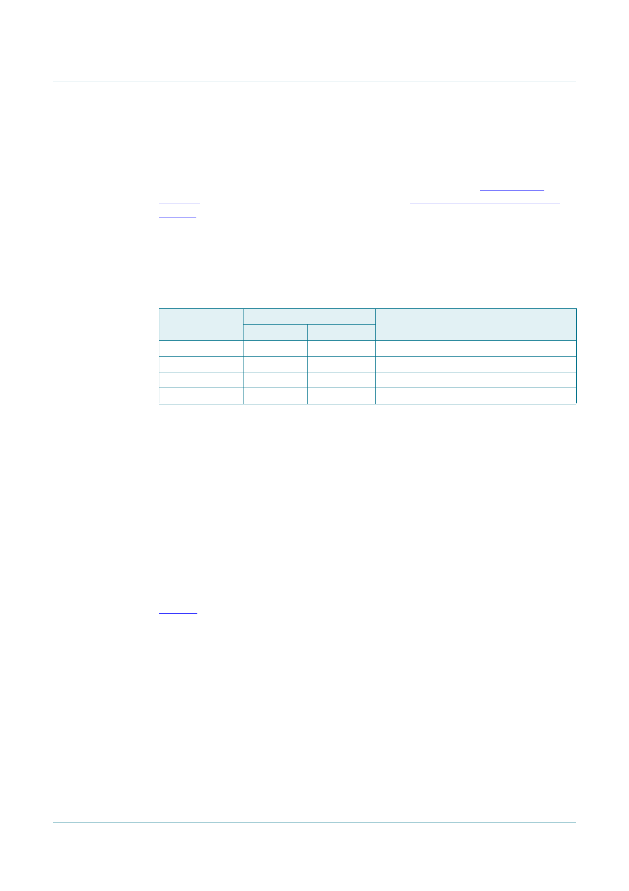
Table 6. Lock bytes
Name
Number
Lock byte 0
2
Lock byte 1
2
Lock byte 2
40
Lock byte 3
40
Page
Address
02h
02h
28h
28h
Function
page and block locking
page locking
page and block locking
functionality and block locking
Due to the built-in bitwise OR operation, this process is irreversible. If a bit is set to “1”, it
cannot be changed back to “0” again. Therefore, before locking the lock bytes, the user
must ensure that the corresponding user memory area and/or configuration bytes are
correctly written.
The configuration written in the lock bytes is active upon the next REQA or WUPA
command.
The single bits of the 4 bytes available for locking incorporate 3 different functions:
• the read-only locking of the single pages or blocks of the user memory area
• the read-only locking of the single bytes of the configuration memory area
• the locking of the lock bits themselves
The mapping of single bits to memory area for the first 64 bytes (512 bits) is shown in
Figure 6.
The bits of byte 2 and 3 of page 02h represent the field-programmable read-only locking
mechanism. Each page from 03h (OTP bits) to 0Fh may be locked individually to prevent
further write access by setting the corresponding locking bit Lx to 1. After locking the page
is read-only memory.
The 3 least significant bits of lock byte 0 of page 2 are the block-locking bits. Bit 2 handles
pages 0Fh to 0Ah, bit 1 pages 09h to 04h and bit 0 page 03h (OTP bits). Once the block
locking bits are set, the locking configuration for the corresponding memory area is frozen.
NTAG203F
Product data sheet
COMPANY PUBLIC
All information provided in this document is subject to legal disclaimers.
Rev. 3.5 — 28 September 2015
220635
© NXP Semiconductors N.V. 2015. All rights reserved.
10 of 30
Share Link: