CDP1823C/3 查看數據表(PDF) - Intersil
零件编号
产品描述 (功能)
生产厂家
CDP1823C/3 Datasheet PDF : 6 Pages
| |||
CDP1823C/3
Write Cycle Dynamic Electrical Specifications tR, tF = 10ns, CL = 50pF (Continued)
LIMITS
+25oC, -55oC
+125oC
PARAMETER
SYMBOL
VDD
(V)
(NOTE 2)
MIN
MAX
(NOTE 2)
MIN
MAX
UNITS
Data Hold Time from MWR (Note 1)
tDH
5
50
-
70
-
ns
Chip Select Setup
tCS
5
210
-
300
-
ns
NOTES:
1. Limits designate 100% testing. All other limits are designer’s parameters under given test conditions and do not represent 100% testing.
2. Minimum timing to allow the indicated function to occur.
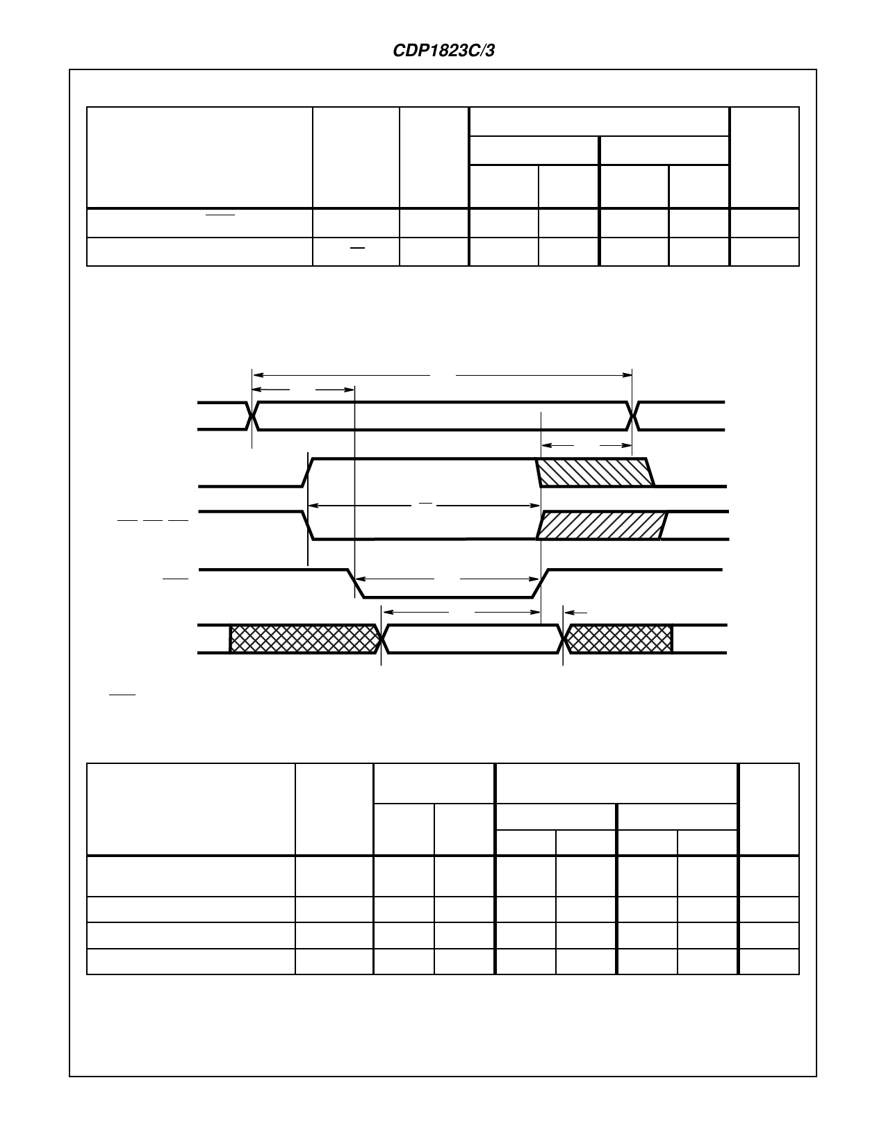
tWC
tAS
ADDRESS
tAH
CS1, CS4
tCS
CS2, CS3, CS5
MWR
BUS 0-7
tWW
tDS
tDH
VALID DATA
NOTE:
1. MRD must be high during write operation.
FIGURE 2. WRITE CYCLE TIMING WAVEFORMS
Data Retention Specifications
PARAMETER
SYMBOL
TEST
CONDITIONS
VDR
(V)
VDD
(V)
LIMITS
+25oC, -55oC
+125oC
MIN
MAX
MIN
MAX
UNITS
Minimum Data Retention Voltage
(Note 1)
VDR
-
-
-
2
-
2.5
V
Data Retention Quiescent Current
IDD
2
-
-
100
-
400
µA
Chip Deselect to Data Retention Time
tCDR
-
5
450
-
650
-
ns
Recovery to Normal Operation Time
tRC
-
5
450
-
650
-
ns
NOTE:
1. Limits designate 100% testing. All other limits are designer’s parameters under given test conditions and do not represent 100% testing.
6-35
Share Link: 