LTC1154 查看數據表(PDF) - Linear Technology
零件编号
产品描述 (功能)
生产厂家
LTC1154 Datasheet PDF : 18 Pages
| |||
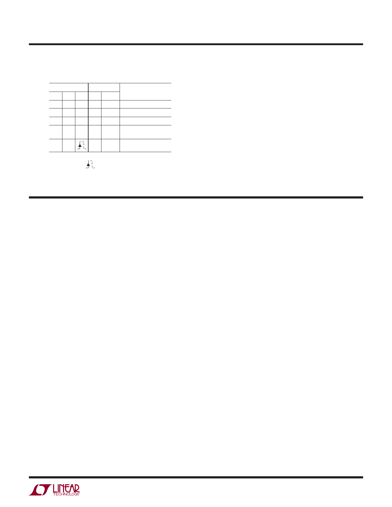
TRUTH TABLE
INPUTS
OUTPUTS
IN EN SD GATE STATUS
SWITCH
CONDITION
XHXL
H
SWITCH OFF
L XXL
H
SWITCH OFF
H L LH
H
SWITCH ON
HLLL
L SWITCH LATCHED OFF
(OVER CURRENT)
HL
L
L SWITCH LATCHED OFF
(SHUTDOWN)
L = LOGIC LOW
H = LOGIC HIGH
X = IRRELEVANT
= EDGE TRIGGERED
LTC1154
The Truth Table demonstrates how the LTC1154 receives
inputs and returns status information to the μP. The
ENABLE and input signal from the μP controls the switch
in its normal operating mode, where the rise and fall
time of the gate drive are controlled to limit EMI and RFI
emissions. The shutdown and overcurrent detection cir-
cuitry however, switch the gate off at a much higher rate
to limit the exposure of the MOSFET switch and the load
to dangerous conditions. The status pin remains high as
long as the switch is operating normally, and is driven
low only when a fault condition is detected. Note that the
shutdown pin is edge-sensitive and latches the output off
even if the shutdown pin returns to a low state.
OPERATION
The LTC1154 is a single micropower MOSFET driver
with built-in protection, status feedback and gate charge
pump. The LTC1154 consists of the following functional
blocks:
TTL and CMOS Compatible Inputs
The LTC1154 input and shutdown input have been designed
to accommodate a wide range of logic families. Both in-
put thresholds are set at about 1.3V with approximately
100mV of hysteresis.
A low standby current voltage regulator provides continu-
ous bias for the TTL-to-CMOS converter. The TTL-to-CMOS
converter output enables the rest of the circuitry. In this
way the power consumption is kept to a minimum in the
standby mode.
ENABLE Input
The ENABLE input is CMOS compatible and inhibits the
input signal whenever it is held logic high. This input
should be grounded when not in use.
Internal Voltage Regulation
The output of the TTL-to-CMOS converter drives two
regulated supplies which power the low voltage CMOS
logic and analog blocks. The regulator outputs are isolated
from each other so that the noise generated by the charge
pump logic is not coupled into the 100mV reference or
the analog comparator.
Gate Charge Pump
Gate drive for the MOSFET switch is produced by an adap-
tive charge pump circuit which generates a gate voltage
substantially higher than the power supply voltage. The
charge pump capacitors are included on chip and there-
fore no external components are required to generate the
gate drive.
Drain Current Sense
The LTC1154 is configured to sense the current flowing
into the drain of the power MOSFET in a high side ap-
plication. An internal 100mV reference is compared to
the drop across a sense resistor (typically 0.002Ω to
0.10Ω) in series with the drain lead. If the drop across
this resistor exceeds the internal 100mV threshold, the
input latch is reset and the gate is quickly discharged via
a large N-channel transistor.
Controlled Gate Rise and Fall Times
When the input is switched ON and OFF, the gate is charged
by the internal charge pump and discharged in a controlled
1154fb
7
Share Link: 