LTC1154 查看數據表(PDF) - Linear Technology
零件编号
产品描述 (功能)
生产厂家
LTC1154 Datasheet PDF : 18 Pages
| |||
LTC1154
OPERATION
manner. The charge and discharge rates have been set to
minimize RFI and EMI emissions in normal operation. If
a short-circuit or current overload condition is encoun-
tered, the gate is discharged very quickly (typically a few
microseconds) by a large N-channel transistor.
Status Output Driver
The status circuitry continuously monitors the fault de-
tection logic. This open-drain output is driven low when
the gate of the MOSFET is driven low by the protection
circuitry. The status circuitry is reset along with the input
latch when the input, or ENABLE input, is cycled.
APPLICATIONS INFORMATION
MOSFET and Load Protection
The LTC1154 protects the power MOSFET switch by remov-
ing drive from the gate as soon as an overcurrent condition
is detected. Resistive and inductive loads can be protected
with no external time delay in series with the drain sense
pin. Lamp loads, however, require that the overcurrent
protection be delayed long enough to start the lamp but
short enough to ensure the safety of the MOSFET.
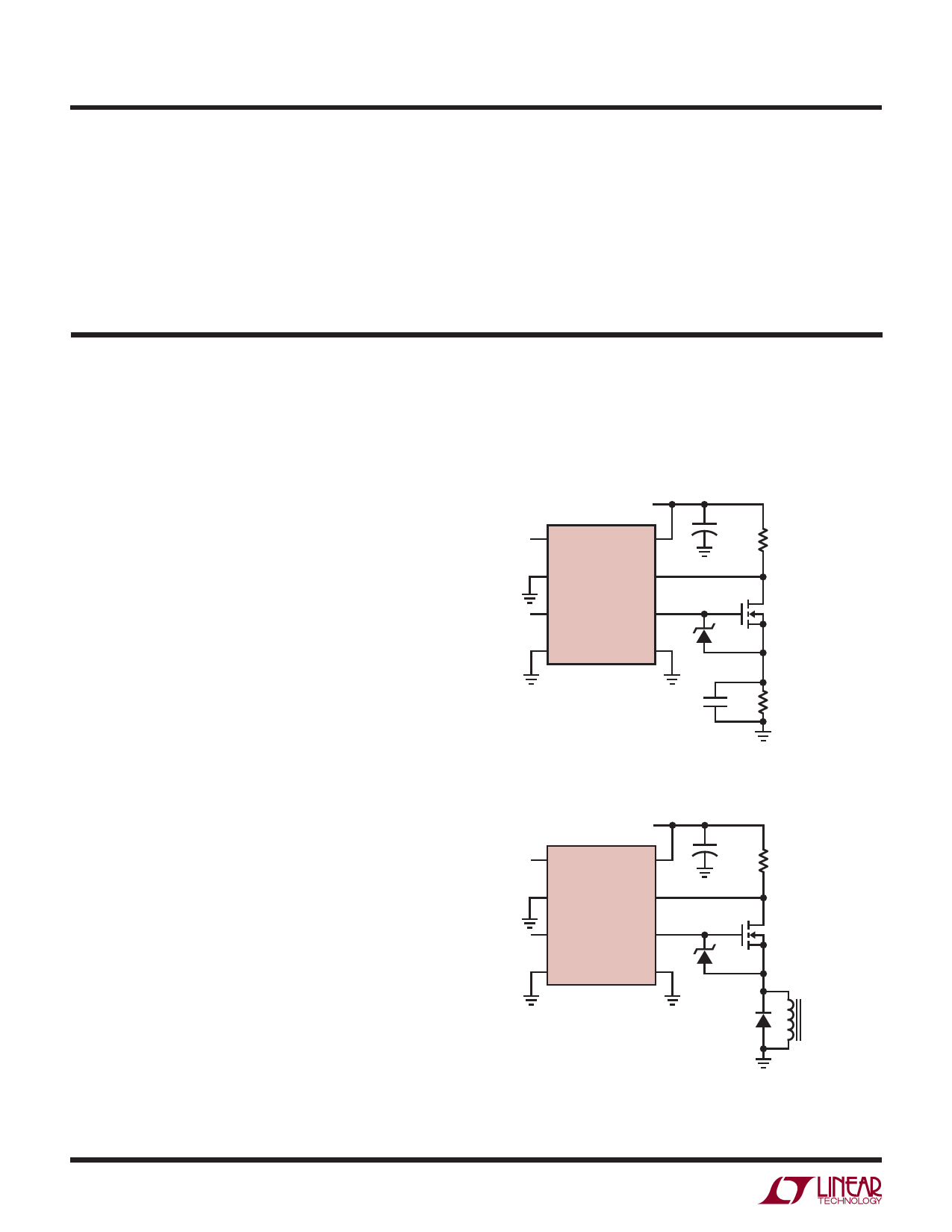
Resistive Loads
Loads that are primarily resistive should be protected with
as short a delay as possible to minimize the amount of time
that the MOSFET is subjected to an overload condition. The
drain sense circuitry has a built-in delay of approximately
10μs to eliminate false triggering by power supply or load
transient conditions. This delay is sufficient to “mask”
short load current transients and the starting of a small
capacitor (<1μF) in parallel with the load. The drain sense
pin can therefore be connected directly to the drain current
sense resistor as shown in Figure 1.
Inductive Loads
Loads that are primarily inductive, such as relays, solenoids
and stepper motor windings should be protected with as
short a delay as possible to minimize the amount of time
that the MOSFET is subjected to an overload condition.
The built-in 10μs delay will ensure that the overcurrent
protection is not false-triggered by a supply or load
transient. No external delay components are required as
shown in Figure 2.
Large inductive loads (>0.1mH) may require diodes con-
nected directly across the inductor to safely divert the
stored energy to ground. Many inductive loads have these
diodes included. If not, a diode of the proper current rating
should be connected across the load, as shown in Figure
2, to safely divert the stored energy.
12V
IN
VS
EN
DS
LTC1154
STATUS
G
GND
SD
+
100μF
0.036Ω
IRFZ24
15V
CLOAD ≤ 1μF
RLOAD
12Ω
LTC1154 • F01
Figure 1. Protecting Resistive Loads
12V
IN
VS
EN
DS
LTC1154
STATUS
G
GND
SD
+
100μF
0.036Ω
IRFZ24
15V
1N5400
12V, 1A
SOLENOID
LTC1154 • F02
Figure 2. Protecting Inductive Loads
1154fb
8
Share Link: 