IDT7025S17PFG(2012) 查看數據表(PDF) - Integrated Device Technology
零件编号
产品描述 (功能)
生产厂家
IDT7025S17PFG Datasheet PDF : 22 Pages
| |||
IDT7025S/L
High-Speed 8K x 16 Dual-Port Static RAM
Military, Industrial and Commercial Temperature Ranges
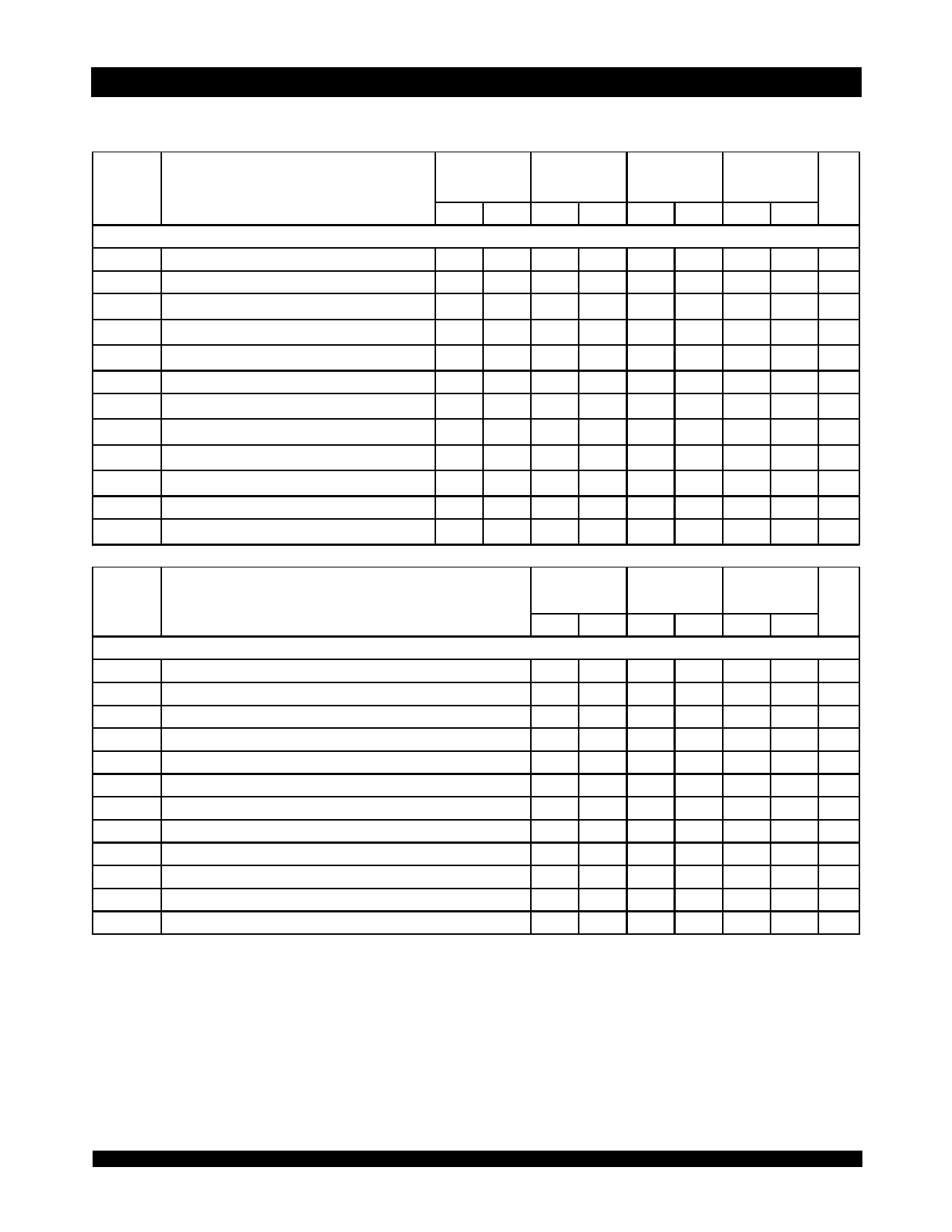
Data Retention Characteristics Over All Temperature Ranges
(L Version Only)
Symbol
Parameter
Test Condition
Min.
Typ.(1)
Max. Unit
VDR
VCC for Data Retention
VCC = 2V
2.0
___
___
V
ICCDR
Data Retention Current
CE > VHC
MIL. & IND.
___
100
4000 µA
VIN > VHC or < VLC
COM'L.
___
100
1500
tCDR(3)
Chip Dese lect to Data Retention Time
SEM > VHC
0
___
___
ns
tR(3)
Operation Recovery Time
tRC(2)
___
___
ns
NOTES:
1. TA = +25°C, VCC = 2V, and are not production tested.
2. tRC = Read Cycle Time
3. This parameter is guaranteed by device characterization, but is not production tested.
4. At Vcc < 2.0V input leakages are undefined.
2683 tbl 10
Data Retention Waveform
DATA RETENTION MODE
VCC
4.5V
VDR ≥ 2V
tCDR
VDR
CE
VIH
4.5V
tR
VIH
AC Test Conditions
Input Pulse Levels
Input Rise/Fall Times
Input Timing Reference Levels
Output Reference Levels
Output Load
GND to 3.0V
5ns Max.
1.5V
1.5V
Figures 1 and 2
2683 tbl 11
DATAOUT
BUSY
INT
347Ω
5V
893Ω
30pF
DATAOUT
347Ω
5V
893Ω
5pF*
2683 drw 05
Figure 1. AC Output Test Load
2683 drw 06
Figure 2. Output Test Load
(for tLZ, tHZ, tWZ, tOW)
* including scope and jig.
6.482
Share Link: 