IDT7025S17PFG(2012) 查看數據表(PDF) - Integrated Device Technology
零件编号
产品描述 (功能)
生产厂家
IDT7025S17PFG Datasheet PDF : 22 Pages
| |||
IDT7025S/L
High-Speed 8K x 16 Dual-Port Static RAM
Military, Industrial and Commercial Temperature Ranges
AC Electrical Characteristics Over the
Operating Temperature and Supply Voltage Range(4)
7025X15
Com'l Only
7025X17
Com'l Only
7025X20
Com'l, Ind
& Military
7025X25
Com'l &
Military
Symbol
Parameter
Min. Max. Min. Max. Min. Max. Min. Max. Unit
READ CYCLE
tRC
Read Cycle Time
tAA
Address Access Time
15
____
17
____
20
____
25
____
ns
____
15
____
17
____
20
____
25
ns
tACE
Chip Enable Access Time(3)
____
15
____
17
____
20
____
25
ns
tABE
Byte Enable Access Time(3)
____
15
____
17
____
20
____
25
ns
tAOE
Output Enable Access Time(3)
____
10
____
10
____
12
____
13
ns
tOH
Output Hold from Address Change
3
____
3
____
3
____
3
____
ns
tLZ
Output Low-Z Time(1,2)
3
____
3
____
3
____
3
____
ns
tHZ
Output High-Z Time(1,2)
____
10
____
10
____
12
____
15
ns
tPU
Chip Enable to Power Up Time (1,2)
0
____
0
____
0
____
0
____
ns
tPD
Chip Disab le to Power Down Time (1,2)
tSOP
Semaphore Flag Update Pulse (OE or SEM)
____
15
____
17
____
20
____
25
ns
10
____
10
____
10
____
10
____
ns
tSAA
Semaphore Address Access(3)
____
15
____
17
____
20
____
25
ns
2683 tbl 12a
7025X35
Com'l &
Military
7025X55
Com'l, Ind
& Military
7025X70
Military Only
Symbol
Parameter
Min. Max. Min. Max. Min. Max. Unit
READ CYCLE
tRC
Read Cycle Time
35
____
55
____
70
____
ns
tAA
Address Access Time
tACE
Chip Enable Access Time(3)
tABE
Byte Enable Access Time(3)
tAOE
Output Enable Access Time(3)
____
35
____
55
____
70
ns
____
35
____
55
____
70
ns
____
35
____
55
____
70
ns
____
20
____
30
____
35
ns
tOH
Output Hold from Address Change
3
____
3
____
3
____
ns
tLZ
Output Low-Z Time(1,2)
3
____
3
____
3
____
ns
tHZ
Output High-Z Time(1,2)
____
15
____
25
____
30
ns
tPU
Chip Enable to Power Up Time (1,2)
0
____
0
____
0
____
ns
tPD
Chip Disab le to Power Down Time (1,2)
____
35
____
50
____
50
ns
tSOP
Semaphore Flag Update Pulse (OE or SEM)
15
____
15
____
15
____
ns
tSAA
Semaphore Address Access(3)
____
35
____
55
____
70
ns
NOTES:
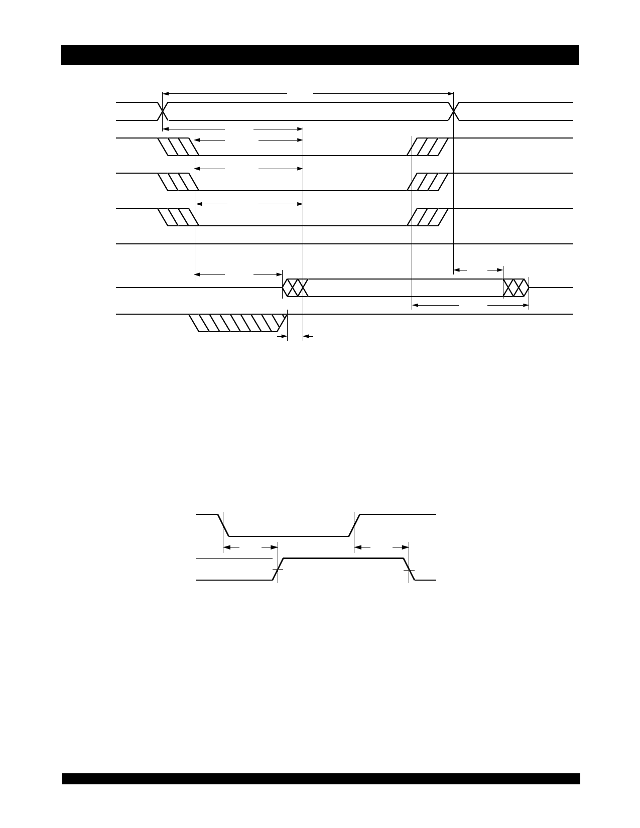
1. Transition is measured 0mV from Low or High-impedance voltage with Output Test Load (Figure 2).
2. This parameter is guaranteed by device characterazation, but is not production tested.
3. To access RAM, CE = VIL, UB or LB = VIL, and SEM = VIH. To access semephore, CE = VIH or UB & LB = VIH, and SEM = VIL.
4. 'X' in part number indicates power rating (S or L).
2683 tbl 12b
6.942
Share Link: 