IDT7015S17GGB 查看數據表(PDF) - Integrated Device Technology
零件编号
产品描述 (功能)
生产厂家
IDT7015S17GGB Datasheet PDF : 20 Pages
| |||
IDT7015S/L
High-Speed 8K x 9 Dual-Port Static RAM
Description:
The IDT7015 is a high-speed 8K x 9 Dual-Port Static RAM. The
IDT7015 is designed to be used as a stand-alone Dual-Port RAM or as
a combination MASTER/SLAVE Dual-Port RAM for 18-bit-or-more word
systems. Using the IDT MASTER/SLAVE Dual-Port RAM approach in 18-
bit or wider memory system applications results in full-speed, error-free
operation without the need for additional discrete logic.
This device provides two independent ports with separate control,
address, and I/O pins that permit independent, asynchronous access for
reads or writes to any location in memory. An automatic power down
Military, Industrial and Commercial Temperature Ranges
feature controlled by CE permits the on-chip circuitry of each port to enter
a very low standby power mode.
Fabricated using IDT’s CMOS high-performance technology, these
devices typically operate on only 750mW of power.
The IDT7015 is packaged in a ceramic 68-pin PGA, a 64-pin PLCC
and an 80-pinTQFP (Thin Quad Flatpack). Military grade product is
manufactured in compliance with the latest revision of MIL-PRF-
38535 QML, making it ideally suited to military temperature applications
demanding the highest level of performance and reliability.
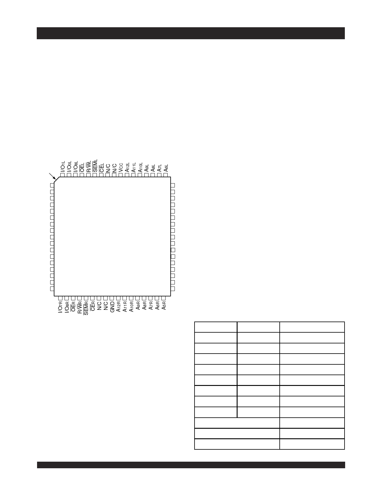
Pin Configurations(1,2,3)
11/16/01
INDEX
I/O2L
I/O3L
I/O4L
I/O5L
GND
I/O6L
I/O7L
VCC
GND
I/O0R
I/O1R
I/O2R
VCC
I/O3R
I/O4R
I/O5R
I/O6R
9 8 7 6 5 4 3 2 1 68 67 66 65 64 63 62 61
10
60
11
59
12
58
13
57
14
56
15
IDT7015J
55
16
J68-1(4)
54
17
53
18
68 Pin PLCC
19
Top View(5)
52
51
20
50
21
49
22
48
23
47
24
46
25
45
26
44
27 28 29 30 31 32 33 34 35 36 37 38 39 40 41 42 43
A5L
A4L
A3L
A2L
A1L
A0L
INTL
BUSYL
GND
M/S ,
BUSYR
INTR
A0R
A1R
A2R
A3R
A4R
NOTES:
1. All VCC pins must be connected to power supply.
2. All GND pins must be connected to ground supply.
3. Package body is approximately .95 in x .95 in x .17 in.
4. This package code is used to reference the package diagram.
5. This text does not imply orientation of Part-marking.
2954 drw 02
Pin Names
Left Port
Right Port
CEL
R/WL
CER
R/WR
OEL
OER
A0L - A12L
A0R - A12R
I/O0L - I/O8L
I/O0R - I/O8R
SEML
SEMR
INTL
INTR
BUSYL
BUSYR
M/S
VCC
GND
6.242
Names
Chip Enable
Read/Write Enable
Output Enable
Address
Data Input/Output
Semaphore Enable
Interrupt Flag
Busy Flag
Master or Slave Select
Power
Ground
2954 tbl 01
APRIL 04, 2006
Share Link: 