IDT7015S17PFB 查看數據表(PDF) - Integrated Device Technology
零件编号
产品描述 (功能)
生产厂家
IDT7015S17PFB Datasheet PDF : 20 Pages
| |||
IDT7015S/L
High-Speed 8K x 9 Dual-Port Static RAM
Capacitance(1)
(TA = +25°C, f = 1.0mhz, for TQFP Package)
Symbol
Parameter
Conditions(2) Max. Unit
CIN Input Capacitance
VIN = 3dV
9 pF
COUT Output Capacitance
VOUT = 3dV
10 pF
NOTES:
2954 tbl 07
1. This parameter is determined by device characteristics but is not
production tested.
2. 3dV references the interpolated capacitance when the input and
output signals switch from 0V to 3V or from 3V to 0V .
Military, Industrial and Commercial Temperature Ranges
DC Electrical Characteristics Over the Operating
Temperature and Supply Voltage Range (VCC = 5.0V ± 10%)
7015S
Symbol
|ILI|
|ILO|
VOL
Parameter
Input Leakage Current(1)
Output Leakage Current
Output Low Voltage
Test Conditions
VCC = 5.5V, VIN = 0V to VCC
CE = VIH, VOUT = 0V to VCC
IOL = +4mA
Min.
Max.
___
10
___
10
___
0.4
VOH
Output High Voltage
IOH = -4mA
2.4
___
NOTE:
1. At Vcc < 2.0V, Input leakages are undefined.
7015L
Min.
Max.
___
5
___
5
___
0.4
2.4
___
Unit
µA
µA
V
V
2954 tbl 08
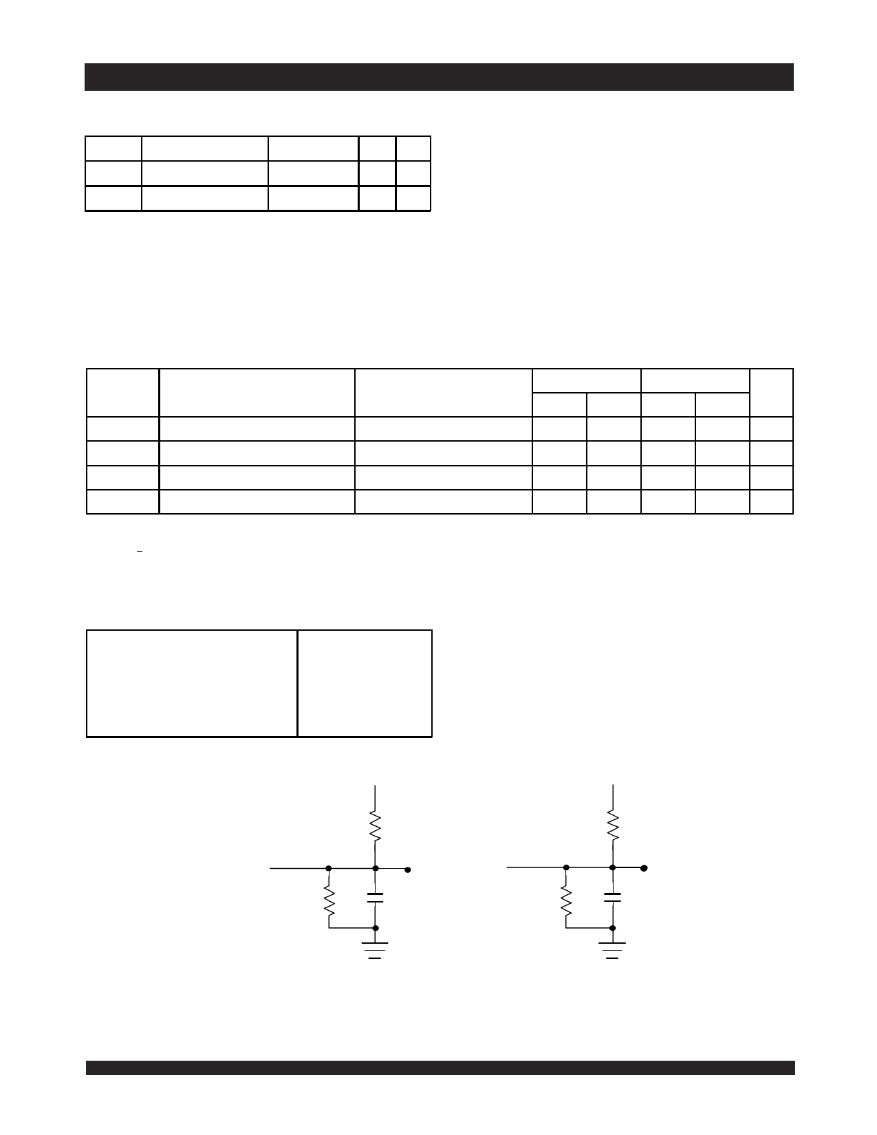
Output Loads and
AC Test Conditions
Input Pulse Levels
Input Rise/Fall Times(1)
Input Timing Reference Levels
Output Reference Levels
Output Load
GND to 3.0V
3ns Max.
1.5V
1.5V
Figures 1 and 2
2954 tbl 09
5V
DATAOUT
BUSY
INT
347Ω
893Ω
30pF
DATAOUT
347Ω
5V
893Ω
5pF *
2954 drw 05
Figure 1. AC Output Test Load
6.542
2954 drw 06
Figure 2. Output Test Load
(For tLZ, tHZ, tWZ, tOW)
*Including scope and jig.
APRIL 04, 2006
Share Link: 