IDT7015S17G 查看數據表(PDF) - Integrated Device Technology
零件编号
产品描述 (功能)
生产厂家
IDT7015S17G Datasheet PDF : 20 Pages
| |||
IDT7015S/L
High-Speed 8K x 9 Dual-Port Static RAM
Military, Industrial and Commercial Temperature Ranges
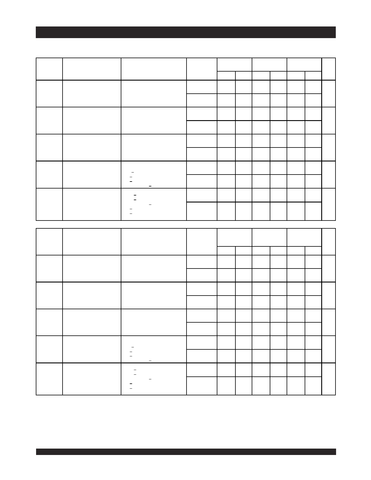
DC Electrical Characteristics Over the Operating
Temperature and Supply Voltage Range(1) (con't.) (VCC = 5.0V ± 10%)
7015X12
Com'l Only
7015X15
Com'l Only
7015X17
Com'l Only
Symbol
Parameter
Test Condition
Version
Typ.(2) Max. Typ.(2) Max. Typ.(2) Max. Unit
ICC
Dynamic Operating Current
CE = VIL, Outputs Disabled
(Both Ports Active)
SEM = VIH
f = fMAX(3)
COM'L S 170 325 170 310 170 310 mA
L 170 275 170 260 170 260
MIL. &
S
____
____
____
____
____
____
IND.
L
____
____
____
____
____
____
ISB1 Standby Current
(Both Ports - TTL
Level Inputs)
CER = CEL = VIH
SEMR = SEML = VIH
f = fMAX(3)
COM'L S
25
70
25
60
25
60 mA
L
25
60
25
50
25
50
MIL. &
S
____
____
____
____
____
____
IND.
L
____
____
____
____
____
____
ISB2 Standby Current
(One Port - TTL
Level Inputs)
CE"A" = VIL and
CE"B" = VIH(5), Active Port
Outputs Disabled, f=fMAX(3)
SEMR = SEML = VIH
COM'L S 105 200 105 190 105 190 mA
L 105 170 105 160 109 160
MIL. &
S
____
____
____
____
____
____
IND.
L
____
____
____
____
____
____
ISB3 Full Standby Current (Both
Ports - All
CMOS Level Inputs)
Both Ports CEL and
CER > VCC - 0.2V
VIN > VCC - 0.2V or
VIN < 0.2V, f = 0(4)
SEMR = SEML >VCC - 0.2V
COM'L S
1.0
15
1.0
15
1.0
15 mA
L
0.2
5
0.2
5
0.2
5
MIL. &
S
____
____
____
____
____
____
IND.
L
____
____
____
____
____
____
ISB4 Full Standby Current
(One Port - All
CMOS Level Inputs)
CE"A" < 0.2V and
CE"B" > VCC - 0.2V(5)
SEMR = SEML >VCC - 0.2V
VIN > VCC - 0.2V or
VIN < 0.2V, Active Port
Outputs Disable d, f = fMAX(3)
COM'L S 100 180 100 170 100 170 mA
L 100 150 100 140 100 140
MIL. &
S
____
____
____
____
____
____
IND.
L
____
____
____
____
____
____
2954 tbl 10
7015X20
Com'l, Ind
& Military
7015X25
Com'l &
Military
7015X35
Com'l &
Military
Symbol
Parameter
Test Condition
Version
Typ.(2) Max. Typ.(2) Max. Typ.(2) Max. Unit
ICC
Dynamic Operating Current
CE = VIL, Outputs Disabled
(Both Ports Active)
SEM = VIH
f = fMAX(3)
COM'L S
160
290
155
265
150
250 mA
L
160
240
155
220
150
210
MIL. & S
160
380
155
340
150
300
IND.
L
160
310
155
280
150
250
ISB1 Standby Current
(Both Ports - TTL
Level Inputs)
CER = CEL = VIH
SEMR = SEML = VIH
f = fMAX(3)
COM'L S
20
60
16
60
13
60 mA
L
20
50
16
50
13
50
MIL. & S
20
80
16
80
13
80
IND.
L
20
65
16
65
13
65
ISB2 Standby Current
(One Port - TTL
Level Inputs)
CE"A" = VIL and
CE"B" = VIH(5), Active Port
Outputs Disabled, f=fMAX(3)
SEMR = SEML = VIH
COM'L S
95
180
90
170
85
155 mA
L
95
150
90
140
85
130
MIL. & S
95
240
90
215
85
190
IND.
L
95
210
90
180
85
160
ISB3 Full Standby Current (Both
Ports - All
CMOS Level Inputs)
Both Ports CEL and
CER > VCC - 0.2V
VIN > VCC - 0.2V or
VIN < 0.2V, f = 0(4)
SEMR = SEML >VCC - 0.2V
COM'L S 1.0
15
1.0
15
1.0
15 mA
L
0.2
5
0.2
5
0.2
5
MIL. & S 1.0
30
1.0
30
1.0
30
IND.
L
0.2
10
0.2
10
0.2
10
ISB4 Full Standby Current
(One Port - All
CMOS Level Inputs)
CE"A" < 0.2V and
CE"B" > VCC - 0.2V(5)
SEMR = SEML >VCC - 0.2V
VIN > VCC - 0.2V or
VIN < 0.2V, Active Port
Outputs Disable d, f = fMAX(3)
COM'L S
90
155
85
145
80
135 mA
L
90
130
85
120
80
110
MIL. & S
90
230
85
200
80
175
IND.
L
90
200
85
170
80
150
NOTES:
2954 tbl 11
1. 'X' in part numbers indicates power rating (S or L)
2. VCC = 5V, TA = +25°C, and are not production tested. ICCDC = 120mA(typ.)
3. At f = fMAX, address and I/O'S are cycling at the maximum frequency read cycle of 1/tRC, and using “AC Test Conditions” of input levels of GND to 3V.
4. f = 0 means no address or control lines change.
5. Port "A" may be either left or right port. Port "B" is the opposite of port "A".
6.642
APRIL 04, 2006
Share Link: 