IDT7015S17G 查看數據表(PDF) - Integrated Device Technology
零件编号
产品描述 (功能)
生产厂家
IDT7015S17G Datasheet PDF : 20 Pages
| |||
IDT7015S/L
High-Speed 8K x 9 Dual-Port Static RAM
Military, Industrial and Commercial Temperature Ranges
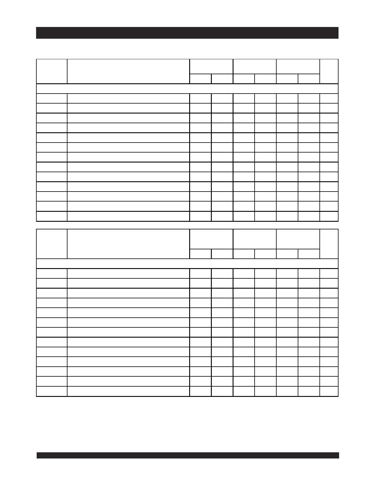
AC Electrical Characteristics Over the
Operating Temperature and Supply Voltage(5)
7015X12
Com'l Only
7015X15
Com'l Only
7015X17
Com'l Only
Symbol
Parameter
Min.
Max.
Min.
Max.
Min.
Max. Unit
WRITE CYCLE
tWC
Write Cycle Time
tEW
Chip Enable to End-of-Write(3)
12
____
15
____
17
____
ns
10
____
12
____
12
____
ns
tAW
Address Valid to End-of-Write
tAS
Address Set-up Time(3)
10
____
12
____
12
____
ns
0
____
0
____
0
____
ns
tWP
Write Pulse Width
10
____
12
____
12
____
ns
tWR
Write Recovery Time
2
____
2
____
0
____
ns
tDW
Data Valid to End-of-Write
tHZ
Output High-Z Time(1,2)
tDH
Data Hold Time(4)
tWZ
Write Enable to Output in High-Z(1,2)
tOW
Output Active from End-of-Write(1,2,4)
10
____
10
____
10
____
ns
____
10
____
10
____
10
ns
0
____
0
____
0
____
ns
____
10
____
10
____
10
ns
3
____
3
____
0
____
ns
tSWRD
SEM Flag Write to Read Time
5
____
5
____
5
____
ns
tSPS
SEM Flag Contention Window
5
____
5
____
5
____
ns
7015X20
Com'l, Ind
& Military
7015X25
Com'l &
Military
7015X35
Com'l &
Military
2954 tbl 13a
Symbol
Parameter
Min.
Max.
Min.
Max.
Min.
Max. Unit
WRITE CYCLE
tWC
Write Cycle Time
tEW
Chip Enable to End-of-Write(3)
20
____
25
____
35
____
ns
15
____
20
____
30
____
ns
tAW
Address Valid to End-of-Write
tAS
Address Set-up Time(3)
15
____
20
____
30
____
ns
0
____
0
____
0
____
ns
tWP
Write Pulse Width
15
____
20
____
25
____
ns
tWR
Write Recovery Time
2
____
2
____
0
____
ns
tDW
Data Valid to End-of-Write
tHZ
Output High-Z Time(1,2)
tDH
Data Hold Time(4)
tWZ
Write Enable to Output in High-Z(1,2)
tOW
Output Active from End-of-Write(1,2,4)
15
____
15
____
15
____
ns
____
12
____
15
____
20
ns
0
____
0
____
0
____
ns
____
12
____
15
____
20
ns
3
____
3
____
3
____
ns
tSWRD
SEM Flag Write to Read Time
5
____
5
____
5
____
ns
tSPS
SEM Flag Contention Window
5
____
5
____
5
____
ns
NOTES:
2954 tbl 13b
1. Transition is measured 0mV from Low- or High-impedance voltage with the Output Test Load (Figure 2).
2. This parameter is guaranteed by device characterization but not tested.
3. To access RAM, CE = VIL and SEM = VIH. To access semaphore, CE = VIH and SEM = VIL. Either condition must be valid for the entire tEW time.
4. The specification for tDH must be met by the device supplying write data to the RAM under all operating conditions. Although tDH and tOW values will vary over voltage
and temperature, the actual tDH will always be smaller than the actual tOW.
5. 'X' in part numbers indicates power rating (S or L).
6.942
APRIL 04, 2006
Share Link: 