M29F512B 查看數據表(PDF) - STMicroelectronics
零件编号
产品描述 (功能)
生产厂家
M29F512B Datasheet PDF : 16 Pages
| |||
M29F512B
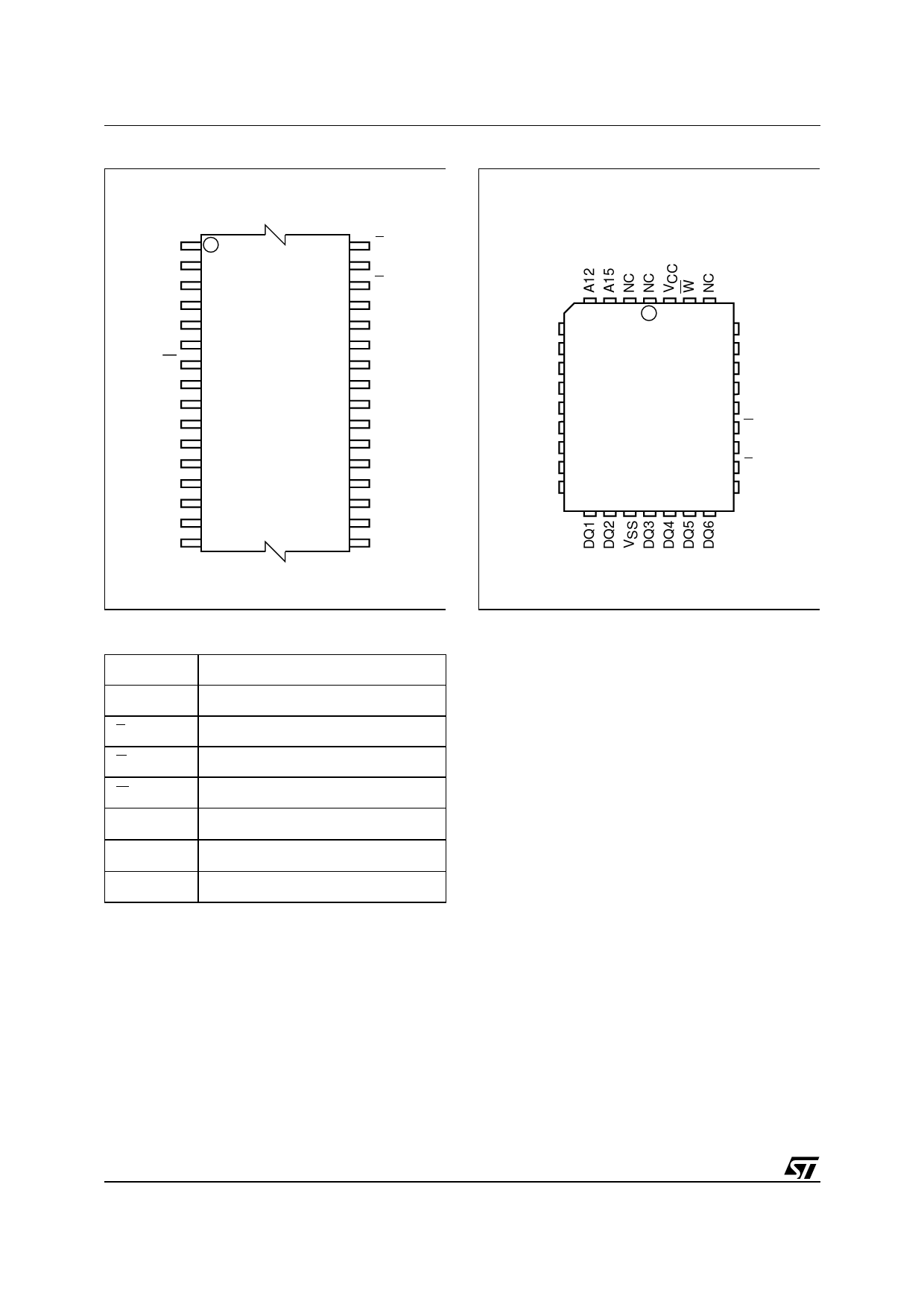
Figure 2A. TSOPConnections
Figure 2B. PLCC Connections
A11
A9
A8
A13
A14
NC
W
VCC
NC
NC
A15
A12
A7
A6
A5
A4
1
32
8 M29F512B 25
9
24
16
17
AI02741
G
A10
E
DQ7
DQ6
DQ5
DQ4
DQ3
VSS
DQ2
DQ1
DQ0
A0
A1
A2
A3
A7
A6
A5
A4
A3 9
A2
A1
A0
DQ0
1 32
M29F512B
17
A14
A13
A8
A9
25 A11
G
A10
E
DQ7
AI02930
Table 1. Signal Names
A0-A15
Address Inputs
DQ0-DQ7 Data Inputs/Outputs
E
Chip Enable
G
Output Enable
W
Write Enable
VCC
Supply Voltage
VSS
Ground
NC
Not Connected Internally
SUMMARY DESCRIPTION
The M29F512B is a 512 Kbit (64Kb x8) non-vola-
tile memory that can be read, erased and repro-
grammed. These operations can be performed
using a single 5V supply. On power-up the memo-
ry defaults to its Read mode where it can be read
in the same way as a ROM or EPROM.
Program and Erase commands are written to the
Command Interface of the memory. An on-chip
Program/Erase Controller simplifies the process of
programming or erasing the memory by taking
care of all of the special operations that are re-
quired to update the memory contents. The end of
a program or erase operation can be detected and
any error conditions identified. The command set
required to control the memory is consistent with
JEDEC standards.
Chip Enable, Output Enable and Write Enable sig-
nals control the bus operation of the memory.
They allow simple connection to most micropro-
cessors, often without additional logic.
The memory is offered in TSOP32 (8 x 14mm) and
PLCC32 packages. Access times of 45ns and
70ns are available. The memory is supplied with
all the bits erased (set to ’1’).
SIGNAL DESCRIPTIONS
See Figure 1, Logic Diagram, and Table 1, Signal
Names, for a brief overview of the signals connect-
ed to this device.
Address Inputs (A0-A15). The Address Inputs
select the cells in the memory array to access dur-
ing Bus Read operations. During Bus Write opera-
tions they control the commands sent to the
Command Interface of the internal state machine.
Data Inputs/Outputs (DQ0-DQ7). The Data In-
puts/Outputs output the data stored at the selected
address during a Bus Read operation. During Bus
Write operations they represent the commands
sent to the Command Interface of the internal state
machine.
2/16
Share Link: 