CXA1843Q 查看數據表(PDF) - Sony Semiconductor
零件编号
产品描述 (功能)
生产厂家
CXA1843Q Datasheet PDF : 20 Pages
| |||
CXA1843Q
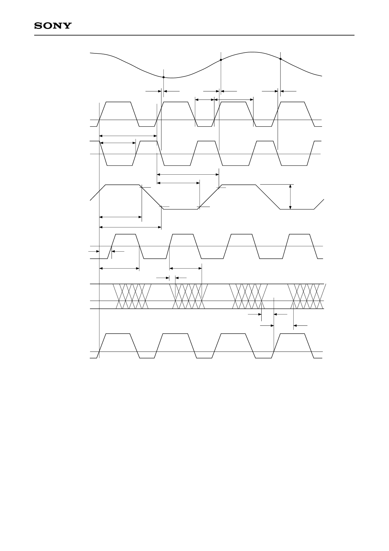
Timing Chart
VIN (Pin 3)
(0 to –2V)
N
Tsd
N+1
Tsd
TPWL
TPWH
N+2
Tsd
MCLK(Pin 31)
(TTL)
S/H CLK
(Not output to outside)
S/H OUT (Pin 11)
(0 to –2V)
T4
T3
Hold
Sample
Hold
Sample
Hold
Sample
Hold
N–1
tdf
taqf
10%
taqr
tdr
N
90%
90%
N+1
10%
2Vp-p N + 2
A/D CLK (Pin 22)
(PECL)
T1 =
6ns
T2
tD (max)
tD (min)
Threshold
voltage =
1.5V
Threshold
voltage
Threshold
voltage =
VCC – 1.2V
A/D output (CXA1844Q)
(TTL)
DN – 3
MCLK
(Clock pulse for the
device next to the ADC
in order to latch the
A/D output)
DN – 2
DN – 1
DN
TS
Th
Threshold
voltage =
1.5V
Threshold
voltage =
1.5V
MCLK:
System master clock.
S/H CLK:
This clock actuates the internal sample-and-hold circuit.
The internal clock pulse circuit generates the S/H CLK, which is not output outside the IC.
A/D CLK:
This clock actuates the A/D converter. The internal clock buffer circuit generates the A/D CLK.
This clock has the level where +5V is shifted from the ECL level.
TPWH, TPWL: S/H CLKIN input clock width
Tsd:
S/H sampling delay for the S/H internal clock
T1:
Fixed time interval between master clock rise and A/D CLK rise, T1 = 6ns (typ.)
T2:
Time interval between MCLK rise and A/D CLK fall
T3:
Time interval between MCLK rise and S/H CLK rise
T4:
Time interval between MCLK rise and S/H CLK fall
taqf, tdf:
10%/90% falling output delay of S/H from MCLK rise
taqr, tdr:
10%/90% rising output delay of S/H from MCLK rise
tD (min., max.): Minimum/maximum output delay of A/D converter (Refer to the CXA1844Q specification.)
Ts:
Setup time of A/D output and MCLK
Th:
Hold time of A/D output and MCLK
–6–
Share Link: 