LC72720YV(2013) 查看數據表(PDF) - ON Semiconductor
零件编号
产品描述 (功能)
生产厂家
LC72720YV Datasheet PDF : 18 Pages
| |||
LC72720YV
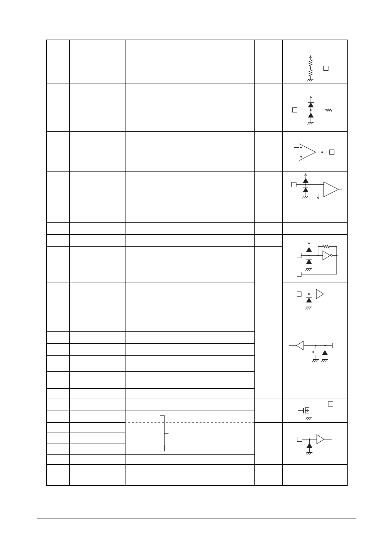
Pin Functions
Pin No.
Pin name
1
VREF
Function
Reference voltage output (Vdda/2)
2
MPXIN
Baseband (multiplexed) signal input
I/O
Output
Input
Pin circuit
Vdda
Vssa
Vdda
Vssa
6
FLOUT
Subcarrier output (filter output)
Output
Vdda
7
CIN
3
Vdda
5
Vssa
15
XOUT
Subcarrier input (comparator input)
Analog system power supply (+3.3V)
Analog system ground
Crystal oscillator output (4.332/8.664MHz)
Input
Vssa
VREF
−
−
Output
XIN
−
−
Vddd
16
XIN
Crystal oscillator input (external reference signal input)
XOUT Vssd
9
T1
10
T2
Test input (This pin must always be connected to ground.)
Test input (standby control)
0:Normal operation, 1:Standby state
(crystal oscillator stopped)
Input
S
Vssd
11
T3(RDCL)
Test I/O (RDS clock output)
13
T4(RDDA)
Test I/O (RDS data output)
14
T5(RSFT)
Test I/O (soft-decision control data output)
T6
20
(ERROR/57K/BE1)
Test I/O (error status, regenerated carrier, error block count)
T7
Test I/O
21
(CORREC/ARI-ID/BE0) (error correction status, SK detection, error block count)
22
SYNC
Block synchronization detection output
I/O*
Vssd
24
RDS-ID
25
DO
RDS detection output
Data output
Serial data interface (CCB)
Output
Vssd
26
CL
28
DI
29
CE
Clock input
Data input
Chip enable
Input
S
Vssd
30
SYR
Synchronization and RAM address reset (active high)
17
Vddd
Digital system power supply (+3.3V)
−
−
18
Vssd
Digital system ground
−
−
Note : * Normally function as an output pin. Used as an I/O pin in test mode, which is not available to user
applications. Pin 4, 8, 12, 19, 23, 27 are NC (NO CONNECT) Pins.
No. 6488-6/18
Share Link: 