LC72720YVS-MPB-E 查看數據表(PDF) - ON Semiconductor
零件编号
产品描述 (功能)
生产厂家
LC72720YVS-MPB-E Datasheet PDF : 19 Pages
| |||
LC72720YVS
Specifications
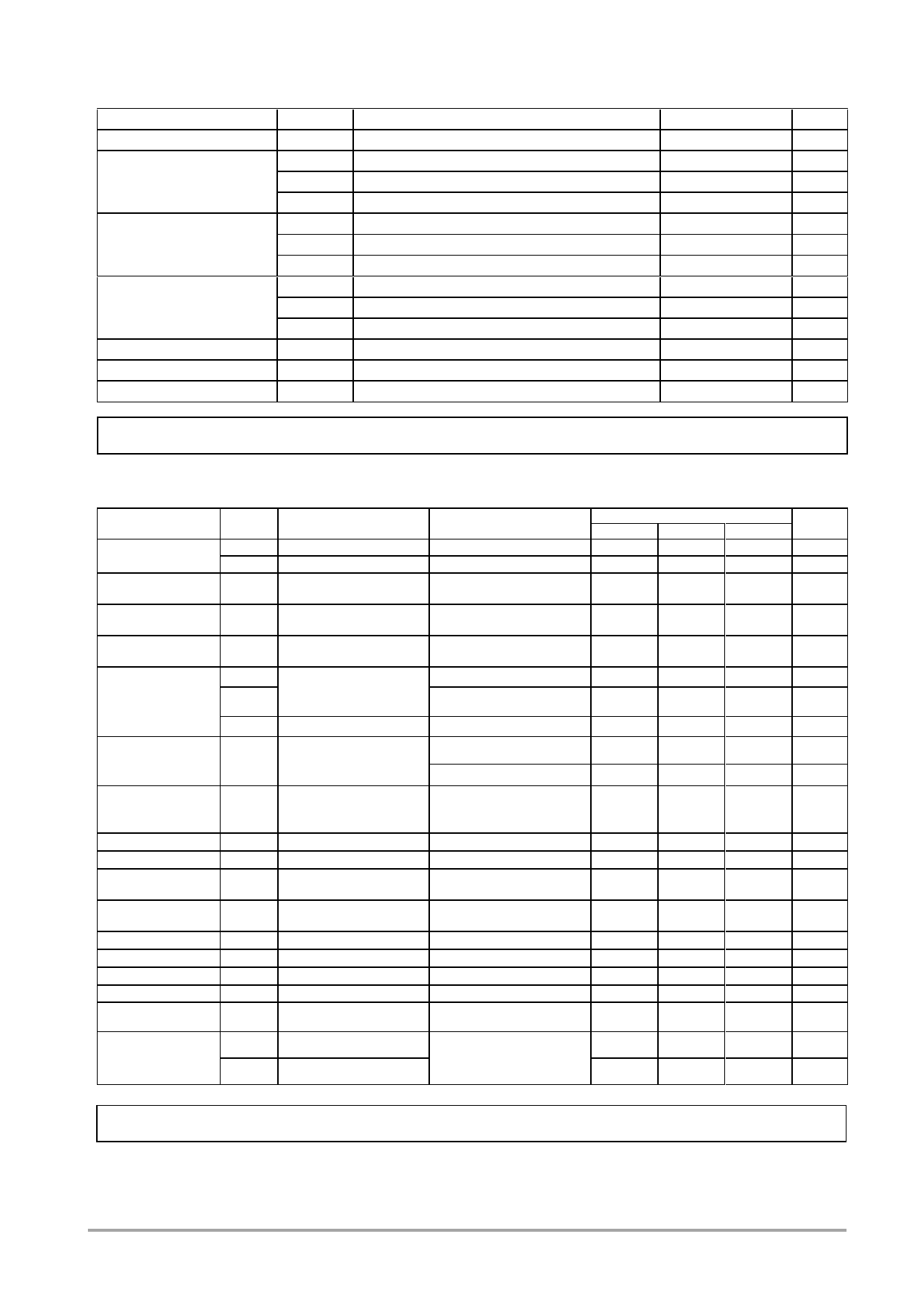
Absolute Maximum Ratings at Ta = 25C, Vssd = Vssa = 0 V
Parameter
Symbol
Pin Name
Maximum supply voltage
Vddmax Vddd, Vdda
Vin1max CL, DI, CE, SYR, T1, T2, T3, T4, T5, T6, T7, SYNC
Maximum input voltage
Vin2max XIN
Vin3max MPXIN, CIN
Vo1max DO, SYNC, RDS-ID, T3, T4, T5, T6, T7
Maximum output voltage
Vo2max XOUT
Vo3max FLOUT
Io1max
DO, T3, T4, T5, T6, T7
Maximum output current
Io2max
XOUT, FLOUT
Io3max
SYNC, RDS-ID
Allowable power dissipation Pdmax
(Ta 85C)
Operating temperature
Topr
Storage temperature
Tstg
Ratings
Unit
0.3 to +7.0
V
0.3 to +7.0
V
0.3 to Vddd+0.3
V
0.3 to Vdda+0.3
V
0.3 to +7.0
V
0.3 to Vddd+0.3
V
0.3 to Vdda+0.3
V
+6.0 mA
+3.0 mA
+20.0 mA
150 mW
40 to +85 C
55 to +125 C
Stresses exceeding those listed in the Maximum Ratings table may damage the device. If any of these limits are exceeded, device functionality should not be assumed,
damage may occur and reliability may be affected.
Allowable Operating Ranges at Ta = 40 to +85C, Vssd = Vssa = 0 V
Parameter
Supply voltage
Input high-level
voltage
Input low-level
voltage
Output voltage
Input amplitude
Guaranteed crystal
Oscillator
frequencies
Crystal oscillator
frequency
deviation
Data setup time
Data hold time
Clock low level
time
Clock high level
time
CE wait time
CE setup time
CE hold time
CE high-level time
Data latch change
time
Data output time
Symbol
Vdd1
Vdd2
VIH
VIL
VO
VIN1
VIN2
VXIN
XTAL
TXtal
tSU
tHD
tCL
tCH
tEL
tES
tEH
tCE
tLC
tDC
tDH
Pin Name
Vddd, Vdda
Vddd
CL, DI, CE, SYR, T1, T2
CL, DI, CE, SYR, T1, T2
DO, SYNC, RDS-ID, T3,
T4, T5, T6, T7
MPXIN
XIN
XIN, XOUT
XIN, XOUT
DI, CL
DI, CL
CL
CL
CE, CL
CE, CL
CE, CL
CE
DO,CL
DO,CE
Conditions
Serial data hold voltage
f = 57 2 kHz
100% modulation
composite
CI 120 Ω (XS = 0)
CI 70 Ω (XS = 1)
fo = 4.332 MHz,
8.664 MHz
Differs depending on the
value of the pull-up
resistor used.
min
3.0
2.0
0.7Vddd
0
100
400
Ratings
typ
4.332
8.664
max
Unit
3.6
V
V
6.5
V
0.3Vddd
V
6.5
50
1500
V
mVrms
mVrms
mVrms
MHz
MHz
100
ppm
0.75
s
0.75
s
0.75
s
0.75
s
0.75
s
0.75
s
0.75
s
20
ms
1.15
s
0.46
s
0.46
s
Functional operation above the stresses listed in the Recommended Operating Ranges is not implied. Extended exposure to stresses beyond the Recommended
Operating Ranges limits may affect device reliability.
www.onsemi.com
2
Share Link: 