LC75878W(2013) 查看數據表(PDF) - ON Semiconductor
零件编号
产品描述 (功能)
生产厂家
LC75878W Datasheet PDF : 35 Pages
| |||
LC75878W
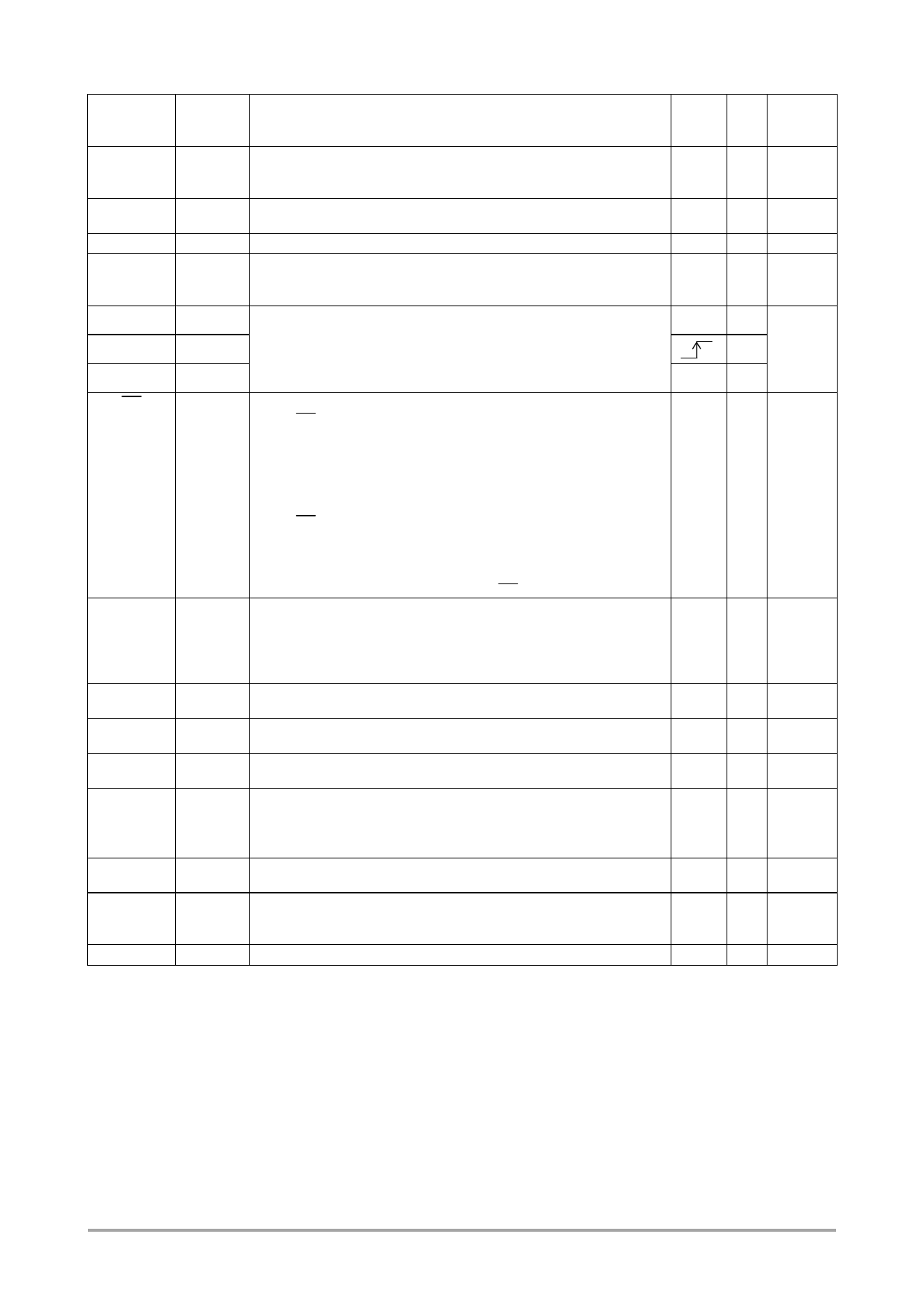
Pin Functions
Symbol
S1 to S73
S74/COM10
S75/COM9
COM1 to
COM8
P1 to P4
Handling
Pin No.
Function
Active I/O
when
unused
1 to 73
Segment driver outputs.
74
The S74/COM10 and S75/COM9 pins can be used as common driver outputs under
-
O
OPEN
75
the control data.
83 to 76 Common driver outputs.
-
O
OPEN
84 to 87 General-purpose output ports.
-
O
OPEN
OSC
CE
CL
DI
INH
VLCD0
VLCD1
VLCD2
VLCD3
VLCD4
VDD
96
Oscillator connection.
An oscillator circuit is formed by connecting an external resistor and capacitor at
this pin.
-
I/O
VDD
98
Serial data transfer inputs.
H
I
These pins are connected to the microcontroller.
99
CE: Chip enable
I
GND
100
CL: Synchronization clock
DI: Transfer data
-
I
97
Input that turns the display off and forces the general-purpose output ports low.
• When INH is low (VSS)
• Display off
S1 to S73 = “L” (VLCD4).
S74/COM10, S75/COM9 = “L” (VLCD4)
COM1 to COM8 = “L” (VLCD4).
• General-purpose output ports P1 to P4 = low (VSS)
• When INH is high (VDD)
• Display on
L
I
GND
• The states of the general-purpose output ports can be set by
the PC1 to PC4 control data.
However, serial data can be transferred when the INH pin is low.
90
LCD drive 4/4 bias voltage (high level) supply pin. The level on this pin can be
changed by the display contrast adjustment circuit.
However, (VLCD0 - VLCD4) must be greater than or equal to 4.5V.
-
Also, external power must not be applied to this pin since the pin circuit includes the
O
OPEN
display contrast adjustment circuit.
91
LCD drive 3/4 bias voltage (middle level) supply pin. This pin can be used to supply
-
the 3/4 (VLCD0 - VLCD4) voltage level externally.
92
LCD drive 2/4 bias voltage (middle level) supply pin. This pin can be used to supply
-
the 2/4 (VLCD0 - VLCD4) voltage level externally.
93
LCD drive 1/4 bias voltage (middle level) supply pin. This pin can be used to supply
-
the 1/4 (VLCD0 - VLCD4) voltage level externally.
94
LCD drive 0/4 bias voltage (low level) supply pin. Fine adjustment of the display
I
OPEN
I
OPEN
I
OPEN
contrast can be implemented by connecting an external variable resistor to this pin.
-
However, (VLCD0 - VLCD4) must be greater than or equal to 4.5V, and VLCD4
must be in the range 0 V to 1.5V, inclusive.
I
GND
88
Logic block power supply connection. Provide a voltage of between 2.7 and 6.0V.
-
-
-
VLCD
VSS
89
LCD driver block power supply connection. Provide a voltage of between 7.0 and
11.0V when the display contrast adjustment circuit is used and provide a voltage of
-
-
-
between 4.5 and 11.0V when the circuit is not used.
95
Power supply connection. Connect to ground.
-
-
-
No.6473-6/35
Share Link: 