LV4924VH жҹҘзңӢж•ёж“ҡиЎЁпјҲPDFпјү - ON Semiconductor
йӣ¶д»¶зј–еҸ·
дә§е“ҒжҸҸиҝ° (еҠҹиғҪ)
з”ҹдә§еҺӮ家
LV4924VH Datasheet PDF : 16 Pages
| |||
LV4924VH
Recommended Operating Range at Ta = 25В°C
Parameter
Recommended supply voltage
range
Recommended PWM pin voltage
Recommended pull-up supply
voltage
Recommended load resistance
Symbol
VD
VIN
Vpup
RL
Conditions
Externally applied voltage
PWM_A1,PWM_A2,PWM_B1,PWM_B2
NPN Open collector pin
Speaker load
min
9
Ratings
typ
13
0
3.3
-
-
4
8
Unit
max
20
V
5
V
18
V
-
О©
Electrical Characteristics Ta=25В°C, VD=13V, RL=8в„Ұ, L=22ОјH (TOKO: A7040HN-220M), C=0.33ОјF (Matsuo: 553M6302-334K)
Parameter
Symbol
Conditions
Ratings
Unit
min
typ
max
Quiescent current
Current at MUTE
Standby current
H input voltage
L input voltage
H input current
L input current
Output pin leakage current
Output pin current
Power Tr ON resistance *1
ICCO
Imute
Ist
VIH
VIL
IIH
IIL
IOFF
IOL
Rds ON
STBY=H, MUTE=H, fIN=384kHz, Duty=50%
STBY=H, MUTE=L, VIN=GND
STBY=L, MUTE=L, VIN=GND
PWM_A, PWM_B, STBY, MUTE
PWM_A, PWM_B, STBY, MUTE
VIN=5V
VIN=GND
NPN Open collector output
OFF-stage 5.0V pull-up
NPN Open collector output
ON-stage, VOL=0.4V
Id=1A
30
2
-
2.3
0
-
-20
-
0.5
-
38
4
-
-
-
-
-
-
-
220
45 mA
6 mA
10 ОјA
5.5
V
1.0
V
60 ОјA
-
ОјA
1 ОјA
-
mA
-
mв„Ұ
Turn ON delay time
td ON
fIN=384kHz, Duty=50%
-
30
50
ns
Turn OFF delay time
td OFF
fIN=384kHz, Duty=50%
-
30
50
ns
Rise-up time
tr
fIN=384kHz, Duty=50%
-
5
20
ns
Fall time
tf
fIN=384kHz, Duty=50%
-
5
20
ns
*1 : The maximum power transistor ON resistance(RDSON) is 270mО©(design guarantee value).
Note : The value of these characteristics were measured in Our test environment. The actual value in an end system will vary depending on the printed circuit
board pattern, the components used, and other factors.
Electrical Characteristics
(Reference value: The table below shows the reference value when FPGA equivalent to the Our reference model is used.)
Parameter
Symbol
Conditions
Ratings
Unit
min
typ
max
Output 1
PO1
THD+N=10%, fIN=1kHz, AES17
-
10
-
W
Output 2
PO2
VD=16V, THD+N=10%, fIN=1kHz, AES17
-
15
-
W
Total harmonic distortion
THD+N
PO=1W, fIN =1kHz, AES17
-
0.1
-
%
Note : The value of these characteristics were measured in Our test environment. The actual value in an end system will vary depending on the printed circuit
board pattern, the components used, and other factors.
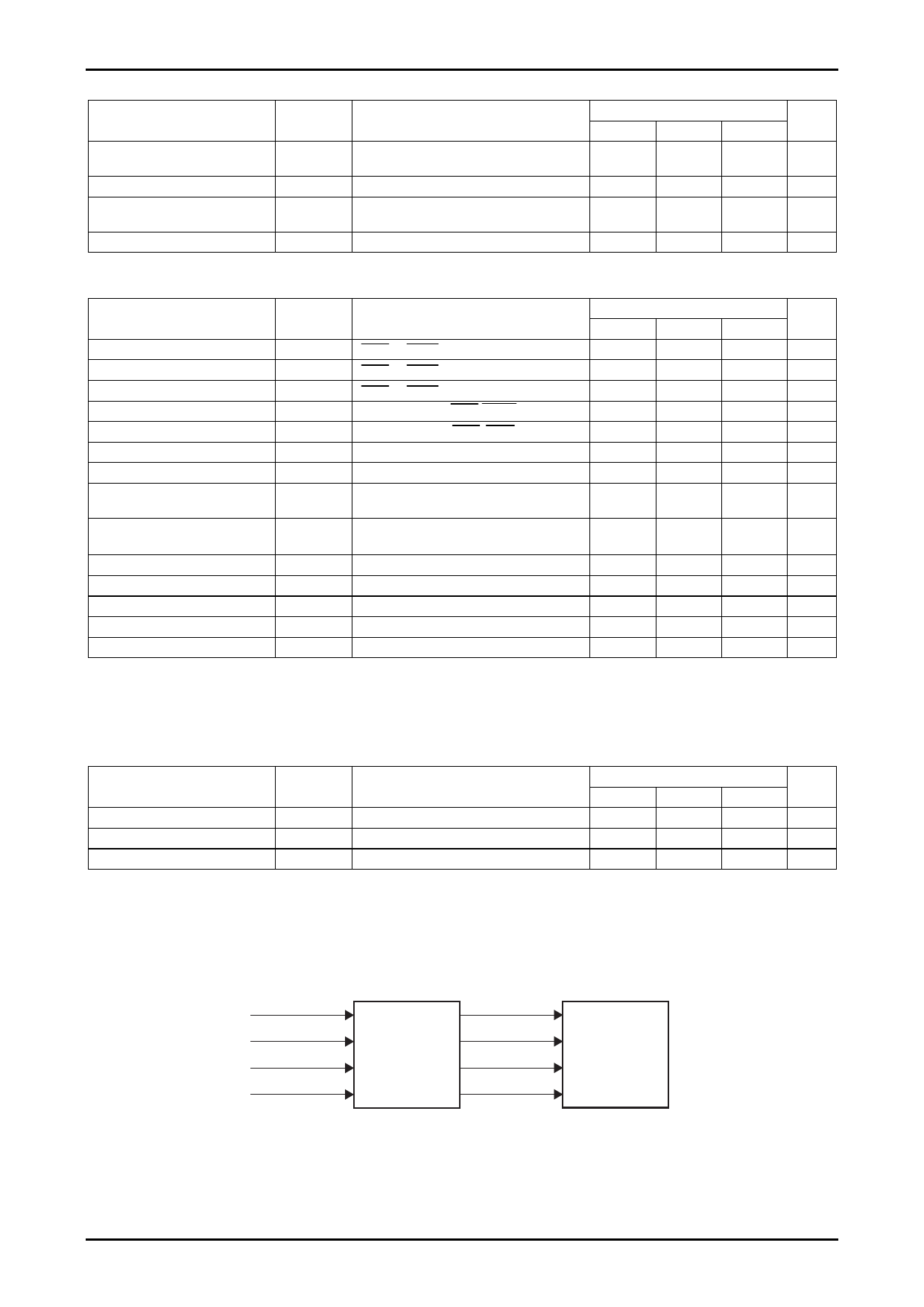
Audio data
IIS
MCLK
BCLK
LRCLK
SDATA
FPGA
PWM BD-mode
MCLK
BCLK
LRCLK
SDATA
LV4924VH
No.A1997-2/15
Share Link: 