M66013FP 查看數據表(PDF) - Renesas Electronics
零件编号
产品描述 (功能)
生产厂家
M66013FP Datasheet PDF : 5 Pages
| |||
M66013FP
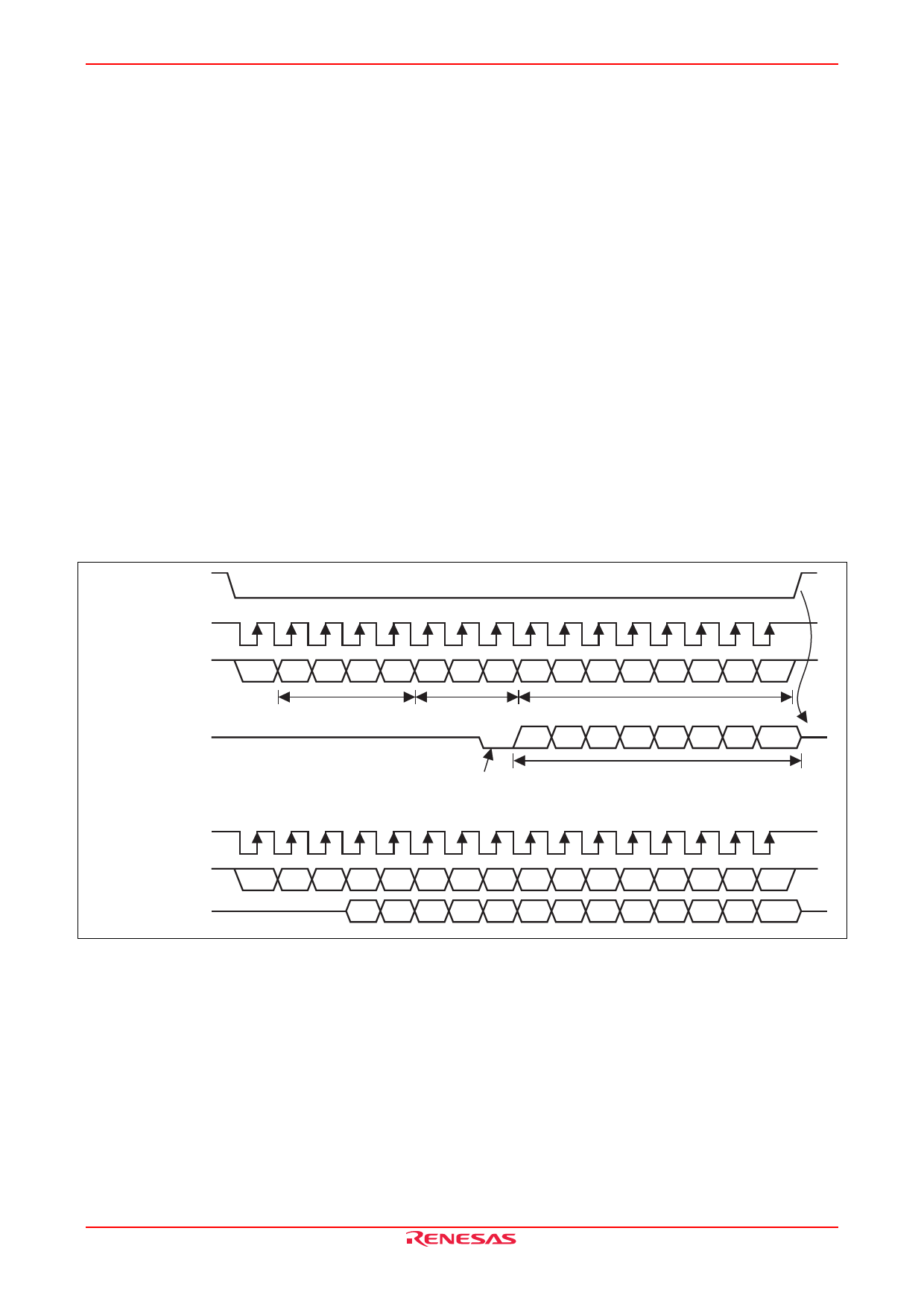
Basic Protocol for Sending and Receiving Data
The following diagram shows the basic protocol for sending and receiving data between the microcomputer and the
M66013.
Falling of EN from "H" to "L" starts a series of sequence and rising of EN from "L" to "H" terminates the sequence.
The concrete operation sequence is as follows:
(1) At a falling edge of EN, 8-bit parallel data of I/O pins D0 to D7 are loaded into the shift register for serial output.
(2) At a rising edge of CLK, DI pin input data is read into the shift register for serial input and the counter for CLK
counts up.
(3) When all address bits are read, a received address is compared with an address set in the address set pin to start the
specified operation only when these addresses matches each other. The DO pin is kept in a high impedance status
until the address comparison is complete.
When these addresses do not match, the DO pin keeps the high impedance status until the next sequence.
(4) When the addresses match each other, the operation for reading serial data from the DI pin and the operation for
output serial data from the D0 pin in synchronization with a falling edge of CLK is carried out.
(5) When 16-bit data has been completely sent or received, the following operations are carried out in synchronization
with a rising edge of EN.
(a) The DO output pin is placed in a high impedance status.
(b) When the CLK counter does not count 16 CLK rising edges, operation (c) below is skipped and the counter is
reset to wait for the next access.
(c) When the counter value is 16, operation for writing to the data register for parallel output, operation for output to
the I/O port or operation for setting/resetting the data setting flag is carried out, and the counter is then reset to
wait for the next address.
EN
CLK
In the
normal mode
DI
DO
1T 2T 3T 4T 5T 6T 7T 8T 9T 10T 11T 12T 13T 14T 15T 16T
X A3 A2 A1 A0 C2 C1 C0 DI7 DI6 DI5 DI4 DI3 DI2 DI1 DI0
Arbitrary
Address bit
Command bit
Data bit
"Z" (High impedance status)
ACK DO7 DO6 DO5 DO4 DO3 DO2 DO1 DO0
"Z"
Acknowledge bit
Data bit
CLK
In the echo
back mode DI
1T 2T 3T 4T 5T 6T 7T 8T 9T 10T 11T 12T 13T 14T 15T 16T
A2 A1 A0 C2 C1 C0 X X DI7 DI6 DI5 DI4 DI3 DI2 DI1 DI0
DO
A2 A1 A0 C1 C0 DO7 DO6 DO5 DO4 DO3 DO2 DO1 DO0
"Z"
"Z"
Figure 1 Basic Protocol (The actual protocol differs depending on the command.)
REJ03F0266-0200 Rev.2.00 Mar 18, 2008
Page 3 of 4
Share Link: 