M66312P 查看數據表(PDF) - Renesas Electronics
零件编号
产品描述 (功能)
生产厂家
M66312P Datasheet PDF : 9 Pages
| |||
M66312P/FP
Functional Description
As M66312 uses silicon gate CMOS process, it realizes high-speed and high-output currents sufficient for LED drive
while maintaining low power consumption and allowance for high noises.
Each bit of a shiftregister consists of two flip-flops having independent clocks for shifting and latching.
As for clock input, shift clock input CKS and latch clock input CKL are independent from each other, shift and latch
operations being made when “L” changes to “H”.
Serial data input A is the data input of the first-step shiftregister and the signal of A shifts shiting registers one by one
when a pulse is impressed to CKS. When A is “H”, the signal of “H” shifts. When A is “L”, the signal of “L” shifts.
When the pulse is impressed to CKL, the contents of the shifting register at that time are stored in a latching register,
and they appear in the output from QA through QH are 3-state outputs.
To extend the number of bits, serial data output SQH is used to output the 8-bit of the shift register.
By connecting CKS and CKL, the shift register state delayed by 1 clock cycle is output at QA through QH.
When reset input R is low, shift register and SQH will be reset. To reset QA through QH to low-level, CKL must be
changed from low-level to high-level after the shift register is reset by R.
When output-enable input OE is high, QA through QH will become high impedance state, but SQH is not changed.
Even if OE is changed, shift operation is not affected.
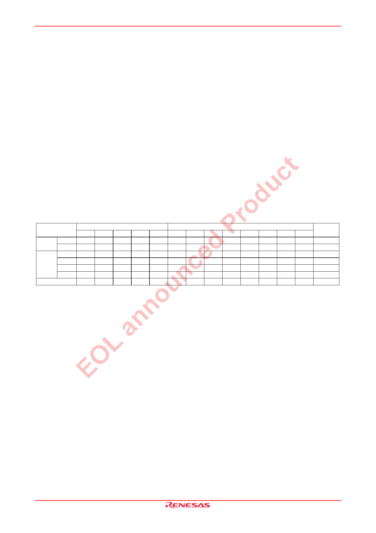
Function Table (Note)
Input
Operation Mode
R
CKS
CKL
A
Reset Shift t1
L
X
X
X
Latch t2 X
X
↑
X
Shift
Shift t1
H
↑
X
H
latch
Latch t2 H
X
↑
X
operation Shift t1
H
↑
X
L
Latch t2 H
X
↑
X
3 state
X
X
X
X
Parallel Data Output
Serial Data
OE
QA
QB
QC
QD
QE
QF
QG
QH Output SQH
L
QA0
QB0
QC0
QD0
QE0
QF0
QG0
QH0
L
L
L
L
L
L
L
L
L
L
L
L
QA0
QB0
QC0
QD0
QE0
QF0
QG0
QH0
qG0
L
H
qA0
qB0
qC0
qD0
qE0
qF0
qG0
qG0
L
QA0
QB0
QC0
QD0
QE0
QF0
QG0
QH0
qG0
L
L
qA0
qB0
qC0
qD0
qE0
qF0
qG0
qG0
H
Z
Z
Z
Z
Z
Z
Z
Z
qH
Note
↑: Change from low-level to high-level
Q0: Output state Q before CKL changed
X: Irrelevant
q0: Contents of shift register before CKS changed
q: Contents of shift register
t1, t2: t2 is set after t1 is set
Z: High impedance
REJ03F0178-0201 Rev.2.01 Mar 31, 2008
Page 3 of 8
Share Link: 