HM6264AFP-10 жҹҘзңӢж•ёж“ҡиЎЁпјҲPDFпјү - Hitachi -> Renesas Electronics
йӣ¶д»¶зј–еҸ·
дә§е“ҒжҸҸиҝ° (еҠҹиғҪ)
з”ҹдә§еҺӮ家
HM6264AFP-10 Datasheet PDF : 10 Pages
| |||
HM6264A Series
Low VCC Data Retention
In data retention mode, CS2 controls the address,
WE, , CS1 OE, and the Din buffer. If CS2 controls
data retention mode, Vin (for these inputs) can be
in the high impedance state. If CS1 controls the
data retention mode, CS2 must satisfy either
HM6264A Series
CS2 вүҘ VCC вҖ“ 0.2 V or CS2 вүӨ 0.2 V. The other
input levels (address, WE, OE, I/O) can be in the
high impedance state.
Low VCC Data Retention Characteristics (Ta = 0 to +70В°C)
This characteristics is guaranteed only L/LL-version.
Parameter
Symbol Min Typ Max Unit Test Condition
VCC for data retention
VDR
2.0
вҖ”
вҖ”
V
CS1 вүҘ VCC вҖ“ 0.2 V,
CS2 вүҘ VCCвҖ“ 0.2 V, or
CS2 вүӨ 0.2 V
Data retention current ICCDR
вҖ”
вҖ”
Chip deselect to data
t
CDR
0
retention time
1*1
50*1 ВөA
VCC = 3.0 V,
CS1 вүҘ VCC вҖ“ 0.2 V,
1*2
25*2
CS2 вүҘ VCC вҖ“ 0.2 V, or
0 V вүӨ CS2 вүӨ 0.2 V, 0 V вүӨ Vin
вҖ”
вҖ”
ns
See retention waveform
Operation recovery time tR
tRC*3
вҖ”
вҖ”
ns
See retention waveform
Notes:
1. VIL min = вҖ“0.3 V, 20 ВөA max at Ta = 0 to 40В°C. These characteristics are guaranteed only for
the L-version.
2. VIL min = вҖ“0.3 V, 10 ВөA max at Ta = 0 to 40В°C. These characteristics are guaranteed only for
the LL-version.
3. tRC = Read cycle time.
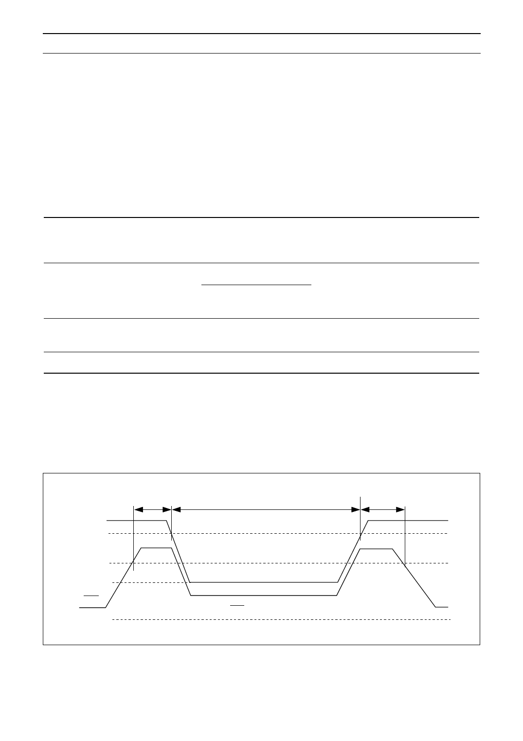
Low VCC Data Retention Waveform (1) (CS1 Controlled)
tCDR
Data retention mode
tR
VCC
4.5 V
2.2 V
VDR
CS1
0V
CS1 вүҘ VCC вҖ“ 0.2 V
9
Share Link: 