MAX174 查看數據表(PDF) - Maxim Integrated
零件编号
产品描述 (功能)
生产厂家
MAX174 Datasheet PDF : 18 Pages
| |||
MAX174/MX574A/MX674A
Industry-Standard, Complete 12-Bit ADCs
PIN
6
7
8
9
10
11
12
13
14
15
16–27
28
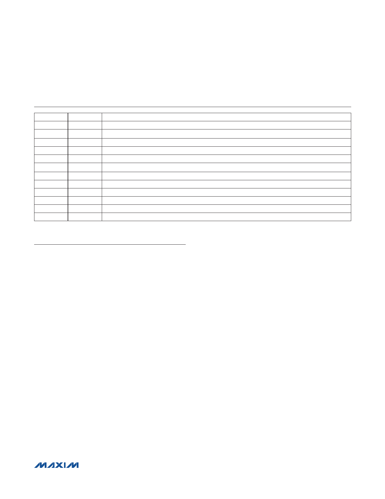
Pin Description (continued)
NAME
CE
VCC
REFOUT
AGND
REFIN
VEE
BIPOFF
10VIN
20VIN
DGND
D0–D11
STS
FUNCTION
Chip-Enable Input. Must be high to select device.
+12V or +15V Supply
+10V Reference Output
Analog Ground
Reference Input
-12V or -15V Supply
Bipolar Offset Input. Connect to REFOUT for bipolar input range.
10V Span Input
20V Span Input
Digital Ground
Three-State Data Outputs
Status Output
Detailed Description
Converter Operation
The MAX174/MX574A/MX674A use a successive approx-
imation technique to convert an unknown analog input to
a 12-bit digital output code. The control logic provides
easy interface to most microprocessors. Most applica-
tions require only a few external passive components to
perform the analog-to-digital (A/D) function.
The internal voltage output DAC is controlled by a suc-
cessive approximation register (SAR) and has an output
impedance of 2.5kω. The analog input is connected to
the DAC output with a 5kω resistor for the 10V input and
10kω resistor for the 20V input. The comparator is essen-
tially a zero-crossing detector, and its output is fed back
to the SAR input.
The SAR is set to half-scale as soon as a conversion starts.
The analog input is compared to 1/2 of the full-scale volt-
age. The bit is kept if the analog input is greater than half-
scale or dropped if smaller. The next bit, bit 10, is then set
with the DAC output either at 1/4 scale, if the most signifi-
cant bit (MSB) is dropped, or 3/4 scale if the MSB is kept.
The conversion continues in this manner until the least
significant bit (LSB) is tried. At the end of the conversion,
the SAR output is latched into the output buffers.
Digital Interface
CE, CS, and R/C control the operation of the MAX174/
MX574A/MX674A. While both CE and CS are asserted,
the state of R/C selects whether a conversion (R/C = 0) or
a data read (R/C = 1) is in progress. The register control
inputs, 12/8 and A0, select the data format and conver-
sion length. A0 is usually tied to the LSB of the address
bus. To perform a full 12-bit conversion, set A0 low during
a convert start. For a shorter 8-bit conversion, A0 must be
high during a convert start.
Output Data Format
During a data read, A0 also selects whether the three
state buffers contain the 8 MSBs (A0 = 0) or the 4 LSBs
(A0 = 1) of the digital result. The 4 LSBs are followed by
4 trailing 0s.
Output data is formatted according to the 12/8 pin. If
this input is low, the output will be a word broken into
two 8-bit bytes. This allows direct interlace to 8-bit buses
without the need for external three-state buffers. If 12/8 is
high, the output will be one 12-bit word. A0 can change
state while a data-read operation is in effect.
To begin a conversion, the microprocessor must write
to the ADC address. Then, since a conversion usually
takes longer than a single clock cycle, the microproces-
sor must wait for the ADC to complete the conversion.
Valid data will be made available only at the end of the
conversion, which is indicated by STS. STS can be ether
polled or used to generate an interrupt upon completion.
Or, the microprocessor can be kept idle by inserting the
appropriate number of No Operation (NOP) instructions
between the conversion-start and data-read commands.
����������������������������������������������������������������� Maxim Integrated Products 8
Share Link: 