V292BMC-33LPN 查看數據表(PDF) - QuickLogic Corporation
零件编号
产品描述 (功能)
生产厂家
V292BMC-33LPN Datasheet PDF : 14 Pages
| |||
V292BMC Rev.D
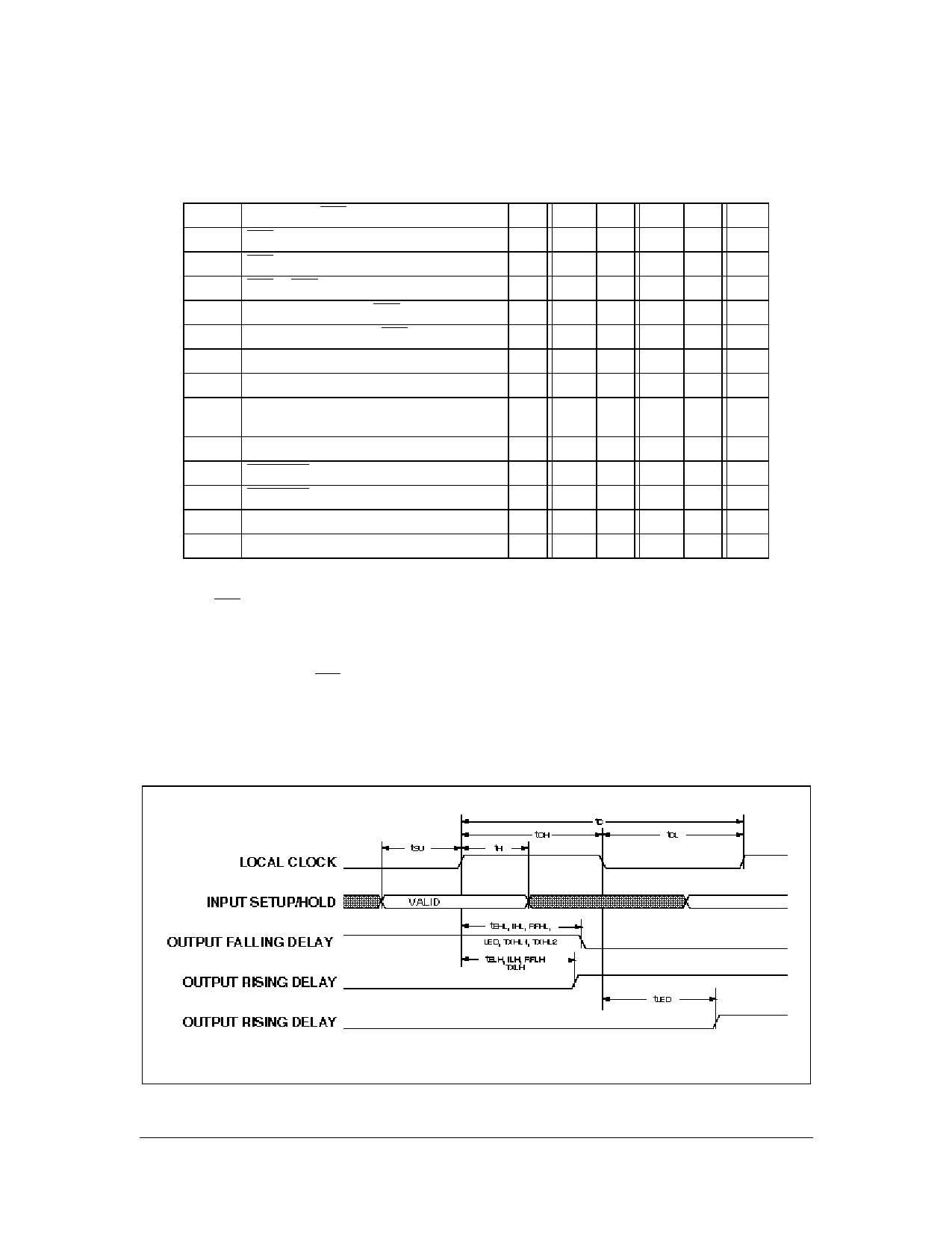
Table 11: Timing Parameters for V292BMC Vcc = 5 Volts +/- 5% (cont’d)and
Vcc3 = 5 or 3.38 Volts +/- 5%
tCLH MEMCLK to CAS de-asserted delay
4 12 3 11 ns
tCAS CAS pulse width
4 tN-1
tN-1
ns
tCPN CAS precharge time
0.5tC
0.5tC
ns
tRCD RAS to CAS delay time
1.5tC-2 1.5tC 1.5tC-2 1.5tC ns
tWESU Write Enable setup to RAS assertion
10
9
ns
tWEH Write Enable hold from RAS de-assertion
1
3
1
3 ns
tLED MEMCLK to Latch Enable output delay
6
3 12 3 10 ns
tTXHL1 MEMCLK to Buffer Control fall delay
7
3 13 3 11 ns
tTXHL2 MEMCLK to Buffer Control fall delay (Mode 2
and 3 at TXA pin only)
4 15 4 13 ns
tTXLH MEMCLK to Buffer Control rise delay
3 12 3 10 ns
tRFHL REFRESH synchronous assertion delay
3 13 3 11 ns
tRFLH REFRESH synchronous de-assertion delay
3 13 3 11 ns
tASU Address setup to ALE Falling
6
5
ns
tAH Address hold from ALE Falling
5
4
ns
NOTES:
1. Specified from MEMCLK falling edge.
2. tM = tC when T_MUX = 1; tM = 0.5 • tC when T_MUX = 0.
3. Maximum RAS pulse width depends on the number of burst access.
4. tN = 1.5 • tC when T_RAS = 0; tN = 2.5 • tC when T_RAS = 1.
5. tP = 2 • tC when T_RAS = 0; tP = 2 • tC when T_RAS = 1 and T_RP = 1;
tP = 3 • tC when T_RAS = 1 and T_RP = 0.
6. Rising delay is measured from MEMCLK falling edge, falling delay is measured from MEMCLK rising edge.
7. Except for Mode 2 and 3 at TXA pin.
8. In order to have 3.3 Volt DRAM interface Vcc3 pins must be connected to 3.3 Volt.
Vcc3 pins are: PIN # 91, 97, 103, 57, 63, 69, 75, 81.
The power supply pins that must always be connected to 5 Volt are Vcc.
Vcc pins are: PIN # 4, 47, 115.
Figure 3: Clock and Synchronous Signals
Copyright © 1998, V3 Semiconductor Corp.
V292BMC Rev D Data Sheet Rev 3.2
11
Share Link: 