V292BMC-33LPN 查看數據表(PDF) - QuickLogic Corporation
零件编号
产品描述 (功能)
生产厂家
V292BMC-33LPN Datasheet PDF : 14 Pages
| |||
V292BMC Rev.D
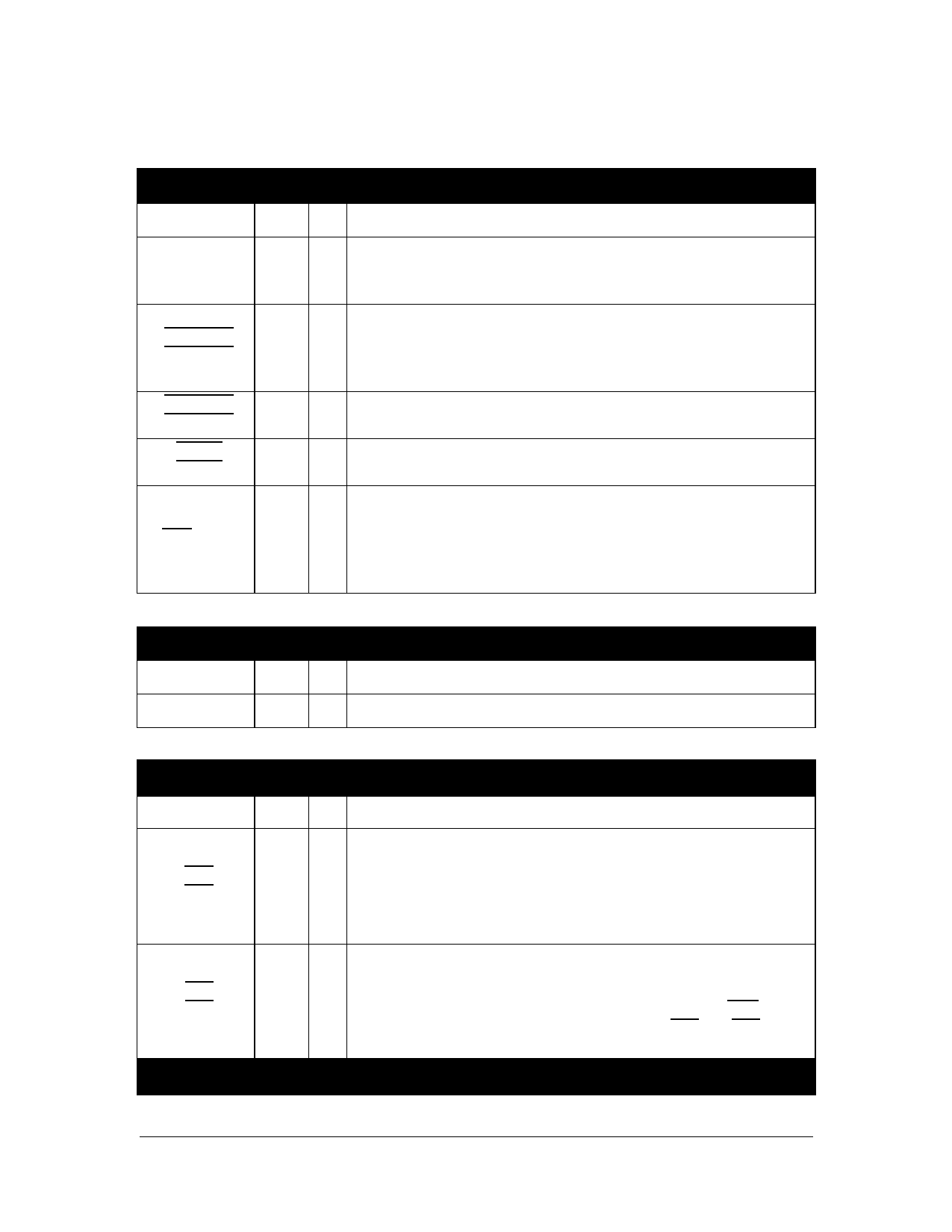
Signal
AA[11:0]
AB[11:0]
RASA[3:0]
RASB[3:0]
CASA[3:0]
CASB[3:0]
MWEA
MWEB
RFS/AUXT
Table 3: Signal Descriptions
Memory Interface Signals
Type Ra
Description
Leaf A and B row and column address, multiplexed on the same
O12-3 X pins. When non-interleaved operation is selected, only address bus
AA should be used.
Row Address Strobe. These strobes indicate the presence of a valid
O12-3 H row address on busses AA(B)[11:0]. These signals are to be con-
nected one to each 32-bit leaf of memory.
O12-3
H
Column Address Strobe. These strobes latch a column address from
AA(B)[11:0]. They are assigned one to each byte in a leaf.
O12-3
H
Memory Write Enable. These are the DRAM write strobes. One is
supplied for each leaf to minimize signal loading.
Refresh in progress. This output is multi-function signal. The signal
name, as it appears on the logic symbol, is the default signal names.
O12 H This signal gives notice that a refresh cycle is to be executed. The
timing leads RAS only refresh by one cycle. The output may also
function as AUX timer interrupt.
Signal
MOD4
Configuration
Type R
Description
I
Selects Modulo 4 (word) bursting for multiplexed address AA(B).
Signal
TXA
TXB
LEA
LEB
Buffer Controls Signals
Type R
Description
Data Transmit A and B. These outputs are multi-function signals.
The signal names, as they appear on the logic symbol, are the
O12
H
default signal names (Mode 0). The purpose of these outputs is to
control buffer output enables during data read transactions and, in
effect, control the multiplexing of data from each memory leaf onto
the Am29030/40 data bus.
These outputs are mode independent, however, the timing of the
signals change for different operational modes. They control trans-
O12
L
parent latches that hold data transmitted during a write transaction.
In modes 0 and 1, the latch controls follow the timing of CAS for
each leaf, while in modes 2 and 3 the timing of LEA and LEB is
shortened to 1/2 clock.
Local Bus Interface
Copyright © 1998, V3 Semiconductor Corp.
V292BMC Rev D Data Sheet Rev 3.2
3
Share Link: 