SZP6SMB51CAT3G(2016) 查看數據表(PDF) - ON Semiconductor
零件编号
产品描述 (功能)
生产厂家
SZP6SMB51CAT3G Datasheet PDF : 7 Pages
| |||
P6SMB11CAT3G Series, SZP6SMB11CAT3G Series
MAXIMUM RATINGS
Rating
Symbol
Value
Unit
Peak Power Dissipation (Note 1) @ TL = 25°C, Pulse Width = 1 ms
PPK
600
W
DC Power Dissipation @ TL = 75°C Measured Zero Lead Length (Note 2)
Derate Above 75°C
Thermal Resistance, Junction−to−Lead
PD
RqJL
3.0
W
40
mW/°C
25
°C/W
DC Power Dissipation (Note 3) @ TA = 25°C
Derate Above 25°C
Thermal Resistance, Junction−to−Ambient
PD
RqJA
0.55
W
4.4
mW/°C
226
°C/W
Operating and Storage Temperature Range
TJ, Tstg
−65 to +150
°C
Stresses exceeding those listed in the Maximum Ratings table may damage the device. If any of these limits are exceeded, device functionality
should not be assumed, damage may occur and reliability may be affected.
1. 10 X 1000 ms, non−repetitive
2. 1″ square copper pad, FR−4 board
3. FR−4 board, using ON Semiconductor minimum recommended footprint, as shown in 403A case outline dimensions spec.
ELECTRICAL CHARACTERISTICS
(TA = 25°C unless otherwise noted)
Symbol
Parameter
IPP
VC
VRWM
IR
VBR
IT
QVBR
Maximum Reverse Peak Pulse Current
Clamping Voltage @ IPP
Working Peak Reverse Voltage
Maximum Reverse Leakage Current @ VRWM
Breakdown Voltage @ IT
Test Current
Maximum Temperature Coefficient of VBR
I
IPP
VC VBR VRWM IIRT
IR
IT
V
VRWM VBR VC
IPP
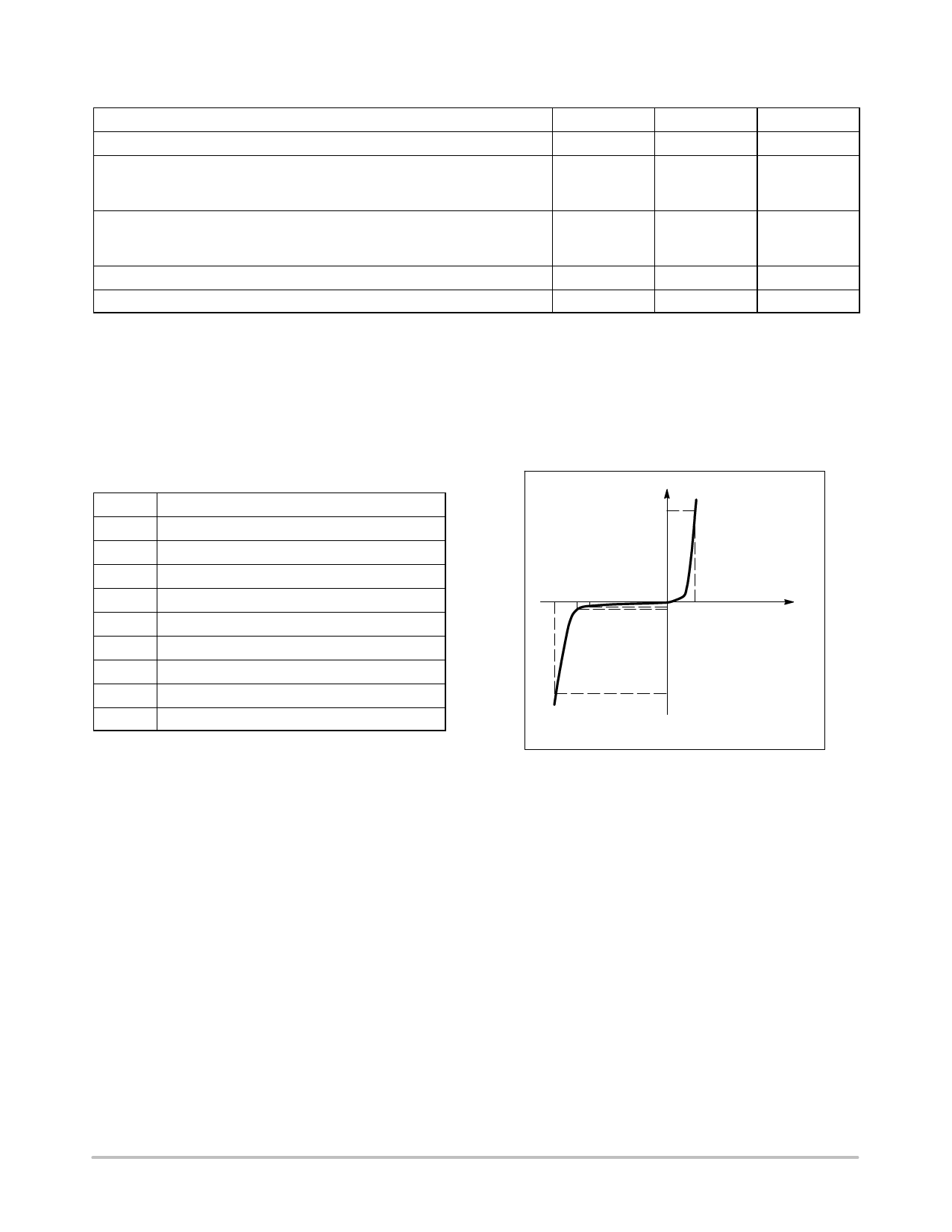
Bi−Directional TVS
ELECTRICAL CHARACTERISTICS (Devices listed in bold, italic are ON Semiconductor Preferred devices.)
Device*
Device
Marking
VRWM
(Note 4)
Volts
IR @
VRWM
mA
Breakdown Voltage
VBR Volts (Note 5)
Min Nom Max
@ IT
mA
VC @ IPP (Note 6)
VC
IPP
Volts Amps
QVBR
%/°C
Ctyp
(Note 7)
pF
P6SMB11CAT3G
P6SMB12CAT3G
11C
9.4
5
10.5 11.05 11.6 1
15.6
38
0.075
865
12C
10.2
5
11.4 12 12.6 1
16.7
36
0.078
800
P6SMB15CAT3G
P6SMB16CAT3G
P6SMB18CAT3G
P6SMB20CAT3G
15C
12.8
5
14.3 15.05 15.8 1
21.2
28
0.084
645
16C
13.6
5
15.2 16 16.8 1
22.5
27
0.086
610
18C
15.3
5
17.1 18 18.9 1
25.2
24
0.088
545
20C
17.1
5
19
20
21
1
27.7
22
0.09
490
P6SMB22CAT3G
P6SMB24CAT3G
P6SMB27CAT3G
P6SMB30CAT3G
22C
18.8
5
20.9 22 23.1 1
30.6
20
0.09
450
24C
20.5
5
22.8 24 25.2 1
33.2
18
0.094
415
27C
23.1
5
25.7 27.05 28.4 1
37.5
16
0.096
370
30C
25.6
5
28.5 30 31.5 1
41.4
14.4
0.097
335
P6SMB33CAT3G
P6SMB36CAT3G
P6SMB39CAT3G
P6SMB43CAT3G
33C
28.2
5
31.4 33.05 34.7 1
45.7
13.2
0.098
305
36C
30.8
5
34.2 36 37.8 1
49.9
12
0.099
280
39C
33.3
5
37.1 39.05 41
1
53.9
11.2
0.1
260
43C
36.8
5
40.9 43.05 45.2 1
59.3
10.1
0.101
240
P6SMB47CAT3G
P6SMB51CAT3G
P6SMB56CAT3G
P6SMB62CAT3G
47C
40.2
5
44.7 47.05 49.4 1
64.8
9.3
0.101
220
51C
43.6
5
48.5 51.05 53.6 1
70.1
8.6
0.102
205
56C
47.8
5
53.2 56 58.8 1
77
7.8
0.103
185
62C
53
5
58.9 62 65.1 1
85
7.1
0.104
170
P6SMB68CAT3G
P6SMB82CAT3G
68C
58.1
5
64.6 68 71.4 1
92
6.5
0.104
155
82C
70.1
5
77.9 82 86.1 1
113
5.3
0.105
130
4. A transient suppressor is normally selected according to the working peak reverse voltage (VRWM), which should be equal to or greater than
the DC or continuous peak operating voltage level.
5. VBR measured at pulse test current IT at an ambient temperature of 25°C.
6. Surge current waveform per Figure 2 and derate per Figure 3 of the General Data − 600 Watt at the beginning of this group.
7. Bias Voltage = 0 V, F = 1 MHz, TJ = 25°C
*Include SZ-prefix devices where applicable.
www.onsemi.com
2
Share Link: 