SFH6318 查看數據表(PDF) - Siemens AG
零件编号
产品描述 (功能)
生产厂家
SFH6318 Datasheet PDF : 3 Pages
| |||
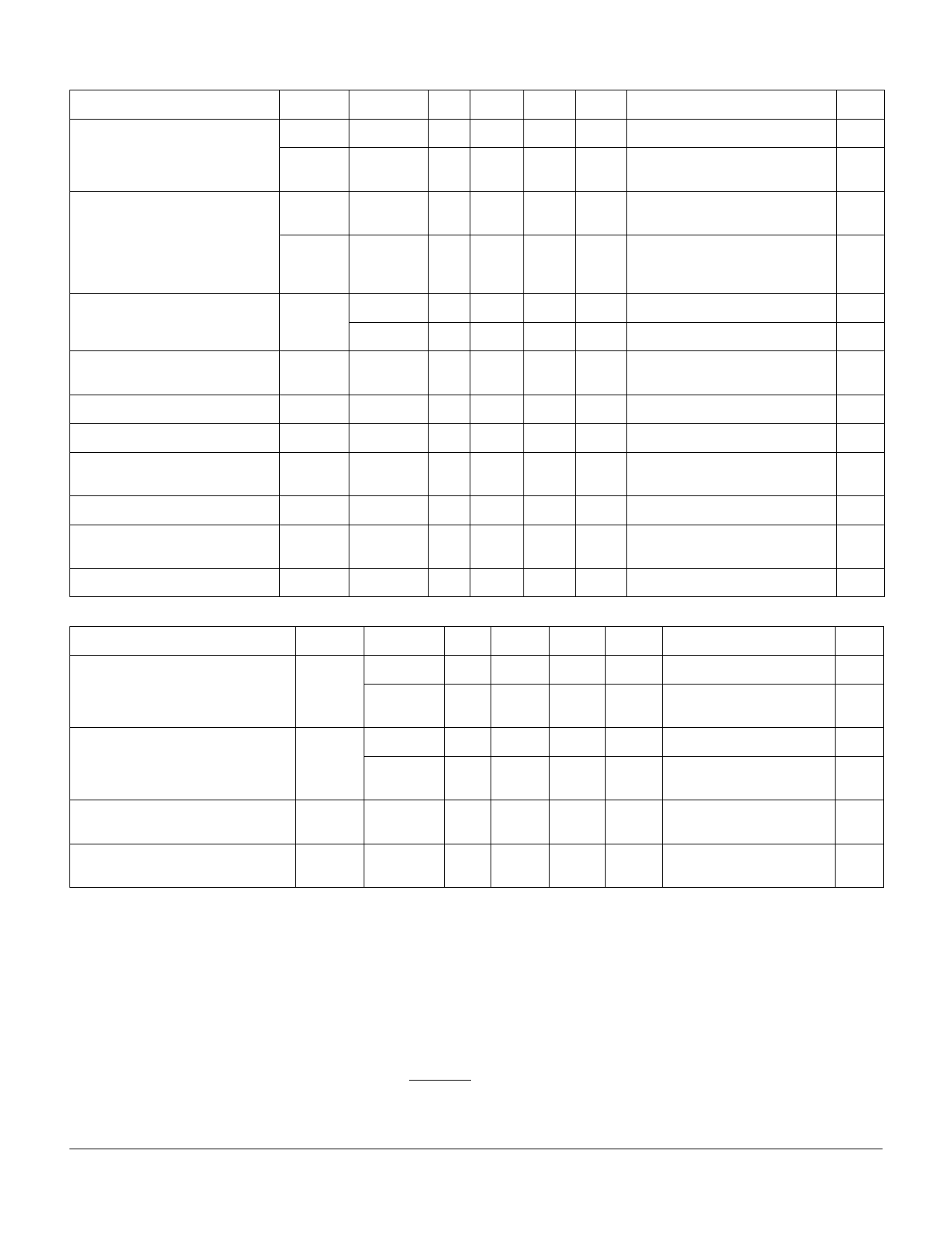
Electro-Optical Characteristics (TA=0°C to 70°C, TA=25°C-Typical, unless otherwise specified)
Parameter
Symbol Device
Min Typ Max Units Test Conditions
Note
Current Transfer Ratio
Logic Low
Output Voltage
CTR
VOL
SFH6318 300 1600 2600 %
SFH6319 400 1600 2600 %
500 2000 3500
SFH6318
0.1
0.4
V
IF=1.6 mA, VO=0.4 V, VCC=4.5 V 1,2
IF=0.5 mA, VO=0.4 V, VCC=4.5 V 1,2
IF=1.6 mA, VO=0.4 V, VCC=4.5 V
IF=1.6 mA, IO=4.8 mA, VCC=4.5 2
V
Logic High
Output Current
Logic Low Supply Current
SFH6319
IOH
ICCL
SFH6318
SFH6319
0.1
0.4
V
0.15 0.4
0.25 0.4
IF=1.6 mA, IO=8 mA, VCC=4.5 V 2
IF=5 mA, IO=15 mA, VCC=4.5 V
IF=12 mA, IO=24 mA, VCC=4.5 V
0.1
250 µA
IF=0 mA, VO=VCC=7 V
2
0.05 100 µA
IF=0 mA, VO=VCC=18 V
2
0.2
1.5
mA IF=1.6 mA, VO=OPEN, VCC=18 2
V
Logic High Supply Current
Input Forward Voltage
Temperature Coefficient,
Forward Voltage
ICCH
VF
∆VF/∆TA
0.01 10
1.4
1.7
–1.8
µA
IF=0 mA, VO=OPEN, VCC=18 V 2
V
IF=1.6 mA, TA=25°C
mV/ IF=1.6 mA
°C
Input Capacitance
CIN
Resistance (Input-Output)
RI-O
Capacitance (Input-Output)
CI-O
Switching Specifications (TA=25°C)
Parameter
Symbol
Device
25
1012
1011
0.6
pF
f=1 MHz, VF=0
Ω
VIO=500 VDC, TA=25°C
Ω
VIO=500 VDC, TA=100°C
pF
f=1 MHz
Min Typ
Max Units Test Conditions
3
3
Note
Propagation Delay Time
To Logic Low at Output
tPHL
SFH6318
SFH6319
2
10
µs
IF=1.6 mA, RL=2.2 KΩ
6
25
µs
IF=0.5 mA, RL=4.7 KΩ
2,4
0.6
1
IF=12 mA, RL=270 Ω
Propagation Delay Time
To Logic High at Output
tPLH
SFH6318
SFH6319
2
35
µs
IF=1.6 mA, RL=2.2 KΩ
4
60
µs
IF=0.5 mA, RL=4.7 KΩ
2,4
1.5
7
IF=12 mA, RL=270 Ω
Common Mode Transient Immunity | CMH |
at Logic High Level Output
1K
V/µs IF=0 mA, RL=2.2 KΩ
5,6
VCM=10 Vp-p
Common Mode Transient Immunity | CML|
at Logic Low Level Output
1K
V/µs IF=1.6 mA, RL=2.2 KΩ
5,6
VCM=10 Vp-p
Notes
1. DC current transfer ratio is defined as the ratio of output collector current, IO, to the forward LED input current, IF times 100%.
2. Pin 7 open.
3. Device considered a two-terminal device: pins 1, 2, 3 and 4 shorted together and pins 5, 6, 7 and 8 shorted together.
4. Using a resistor between pin 5 and 7 will decrease gain and delay time.
5. Common mode transient immunity in logic high level is the maximum tolerable (positive) dVcm/dt on the leading edge of the common mode pulse,
VCM, to assure that the output will remain in a logic high state (i.e. VO>2.0 V) common mode transient immunity in logic low level is the maximum
tolerable (negative) dVcm/dt on the trailing edge of the common mode pulse signal, VCM, to assure that the output will remain in a logic low state
(i.e. VO<0.8 V).
6. In applications where dv/dt may exceed 50,000 V/µs (such as state discharge) a series resistor, RCC should be included to protect IC from destruc
tively high surge currents. The recommended value is RCC≅
IV kΩ. Refer to Figure 2.
0.15 IF(mA)
SFH6318/6319
2
Share Link: 