STK672-740A-E 查看數據表(PDF) - ON Semiconductor
零件编号
产品描述 (功能)
生产厂家
STK672-740A-E Datasheet PDF : 19 Pages
| |||
STK672-740A-E
Specifications
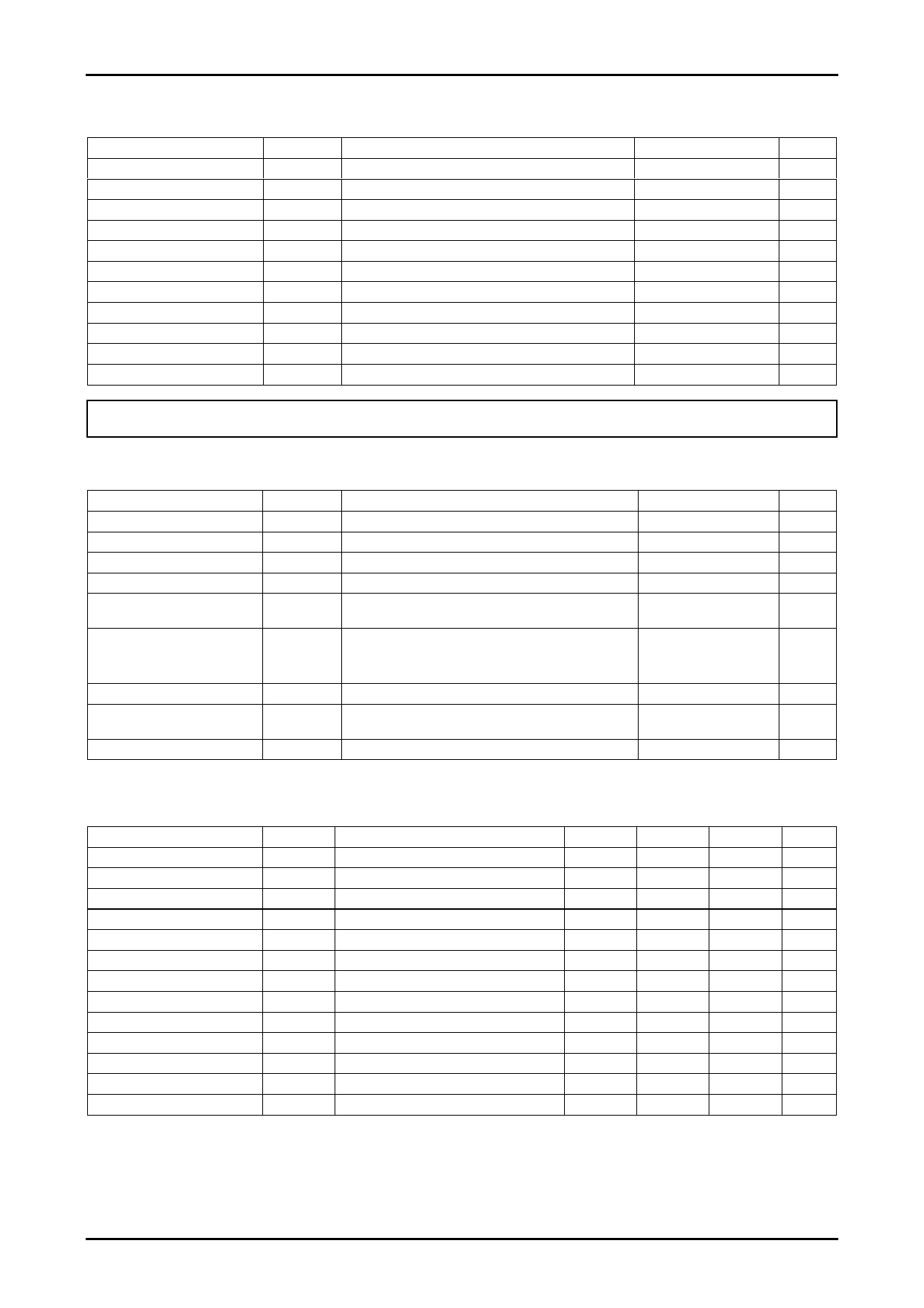
Absolute Maximum Ratings at Tc = 25°C
Parameter
Maximum supply voltage 1
Maximum supply voltage 2
Input voltage
Output current 1
Output current 2
Output current 3
Allowable power dissipation 1
Allowable power dissipation 2
Operating substrate temperature
Junction temperature
Storage temperature
Symbol
VCC max
VDD max
VIN max
IOP max
IOH max
IOF max
PdMF max
PdPK max
Tc max
Tj max
Tstg
Conditions
No signal
No signal
Logic input pins
10µs, 1 pulse (resistance load)
VDD=5V, CLOCK≥200Hz
Pin16 output current
With an arbitrarily large heat sink. Per MOSFET
No heat sink
Ratings
unit
52
V
-0.3 to +6.0
V
-0.3 to +6.0
V
20
A
4
A
10
mA
8.3
W
3.1
W
105
°C
150
°C
-40 to +125
°C
Stresses exceeding Maximum Ratings may damage the device. Maximum Ratings are stress ratings only. Functional operation above the Recommended Operating
Conditions is not implied. Extended exposure to stresses above the Recommended Operating Conditions may affect device reliability.
Allowable Operating Ranges at Ta=25°C
Parameter
Symbol
Conditions
Ratings
unit
Operating supply voltage 1
VCC
With signals applied
10 to 42
V
Operating supply voltage 2
VDD
With signals applied
5±5%
V
Input high voltage
Input low voltage
VIH
Pins 13, 17, 12, 10, 14, 15
VIL
Pins 13, 17, 12, 10, 14, 15
2.5 to VDD
V
0 to 0.8
V
Output current 1
IOH1
Tc=105°C, CLOCK≥200Hz,
Continuous operation, duty=100%
3.0
A
Output current 2
IOH2
Tc=80°C, CLOCK≥200Hz,
Continuous operation, duty=100%,
See the motor current (IOH) derating curve
3.3
A
Phase driver withstand voltage
VDSS
ID=1mA (Tc=25°C)
100min
V
Recommended operating
substrate temperature
Tc
No condensation
0 to 105
°C
Recommended Vref range
Vref
Tc=105°C
0.14 to 1.31
V
Refer to the graph for each conduction-period tolerance range for the output current and brake current.
Electrical Characteristics at Tc=25°C, VCC=24V, VDD=5.0V
Parameter
Symbol
Conditions
min
typ
VDD supply current
ICCO
Pin 9 current CLOCK=GND
4.4
Output average current
Ioave
R/L=1Ω/0.62mH in each phase
0.519
0.625
FET diode forward voltage
Vdf
If=1A (RL=23Ω)
0.83
Output saturation voltage
Vsat
RL=23Ω
0.20
Input high voltage
VIH
Pins 13, 17, 12, 10, 14, 15
2.5
Input low voltage
VIL
Pins 13, 17, 12, 10, 14, 15
FAULT low output voltage
VOLF
Pin 16 (IO=5mA)
0.25
5V level FAULT leakage current
IILF
Pin 16=5V
5V level input current
IILH
Pins 13, 17, 12, 10, 14, 15=5V
50
GND level input current
IILL
Pins 13, 17, 12, 10, 14, 15=GND
Vref input bias current
IIB
Pin 19=1.0V
10
PWM frequency
fc
29
45
Overheat detection temperature
TSD
Design guarantee
144
*Ioave values are for when the lead frame of the product is soldered to the mounting substrate.
Notes: A fixed-voltage power supply must be used.
max
unit
8
mA
0.731
A
1.5
V
0.33
V
V
0.8
V
0.5
V
10
µA
75
µA
10
µA
15
µA
61 kHz
°C
No. A1136-2/19
Share Link: 