NX25F011B 查看數據表(PDF) - Unspecified
零件编号
产品描述 (功能)
生产厂家
NX25F011B Datasheet PDF : 37 Pages
| |||
NX25F011B
NX25F021B
NX25F041B
suspend a command, HOLD must be brought low while
CS and SCK are low. With HOLD low, further data on the
SI pin is ignored (even while SCK is clocked) and the SO
pin goes to a high-impedance state. To resume the
command sequence, HOLD must be brought high when
CS and SCK are low. See timing diagrams.
Status Register Bit Descriptions
The status register provides status of the Flash array’s
Ready/Busy condition (R/B), transfers between the SRAM
and program buffer (TX), Write-Enable/Disable (WE), and
Compare Not Equal (CNE). The register can be read using
the Read Status Register command (Figure 8).
Ready/Busy Status, BUSY
The BUSY status bit is located at bit ST[7] of the status
register. Testing the BUSY bit is one of several ways to
check Ready/Busy status of the array. At power-up the
BUSY bit is reset to 0.
BUSY=1 The device is busy programming.
BUSY=0 The deivce is ready for further use.
SRAM Transfer All or Compare All, TR
The TR status bit is located at bit ST[6] of the status
register. The bit provides status primarily for use during
the Transfer All Sector to SRAM command and Compare
All Sector to SRAM command. An active state 1 indi-
cates a transfer is in process and the SRAM Array is not
available for use. The device will indicate a BUSY state
while the TR bit is active. Upon power up the TR bit resets
to 0.
TR=1 Transfer or Compare All in Process.
TR=0 Transfer or Compare All not in Process.
Write Enable/Disable, WE
The WE status bit is located at bit ST[4] of the status
register. The bit provides write protect status of global Write
Enable and Write Disable commands. Upon power- up the
WE bit resets to 0.
WE=1 Write Enabled, array can be written to.
WE=0 Write Disabled, array can not be written to.
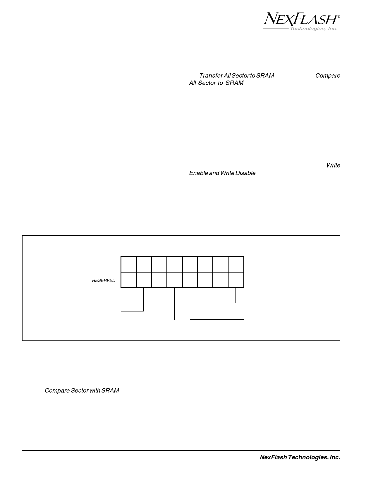
ST7 ST6 ST5 ST4 ST3 ST2 ST1 ST0
x =RESERVED Busy TR X WE CNE X X PD
READ/BUSY
SRAM TRANSFER OR COMPARE
FLASH ARRAY WRITE ENABLE/DISABLE
POWER DETECT
SECTOR-SRAM COMPARE NOT EQUAL
Figure 8. Status Register Bit Locations
Compare Not Equal, CNE
The CNE status bit is located at bit ST[3] of the status
register. The bit provides a cumulative comparison result
during a Compare Sector with SRAM command. The CNE
bit is reset to a 0 upon power-up or after a Clear Compare Bit
command is executed.
CNE=1 Sector and SRAM contents are not equal.
CNE=0 Sector and SRAM are equal or CNE bit reset.
Power Detect, PD
The Power Detect bit works in conjunction with the Set
Power Detection and Reset Power Detection Commands
and is primarily used for removable media applications. The
Set Power Detect Command must be issued before the PD
bit can be used for power detection.
PD=0 Power has been removed
PD=1 Power has not been removed
12
NexFlash Technologies, Inc.
PRELIMINARY NXSF016F-1201
12/12/01 ©
Share Link: 