NX25F011B 查看數據表(PDF) - Unspecified
零件编号
产品描述 (功能)
生产厂家
NX25F011B Datasheet PDF : 37 Pages
| |||
NX25F011B
NX25F021B
NX25F041B
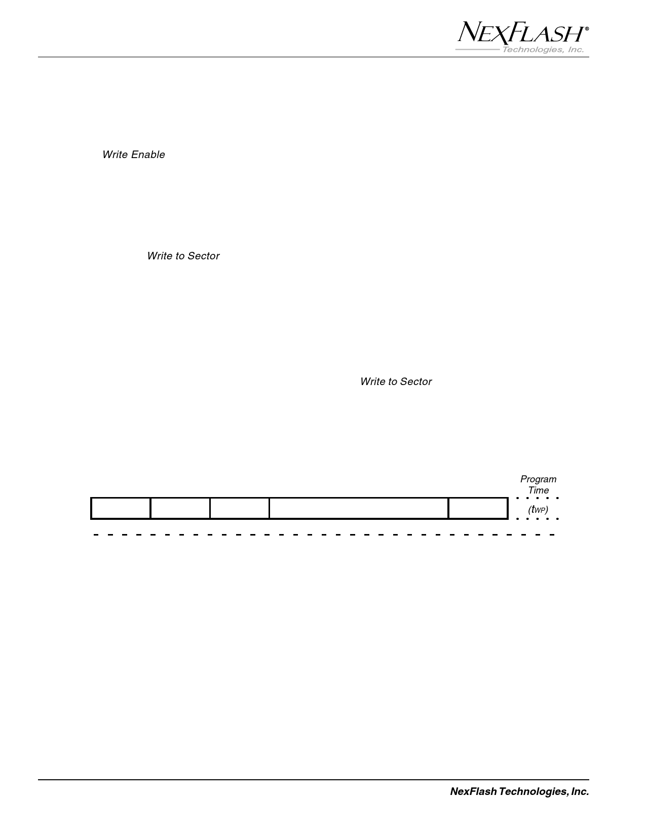
Write to Sector Through SRAM (F3H)
Before writing to a sector in the Flash memory array, all
hardware and software write protection must be in an
enabled state. This means that the WP pin must be in a
high state, a Write Enable command must have previ-
ously been issued, and the sector location that is to be
written to must be outside the write protect range set in
the configuration register. Additionally, the Ready/Busy
status should be checked to confirm that the memory
array is available to be written to.
Writing to a sector is accomplished by first bringing CS
low and shifting in the Write to Sector command (F3H)
followed by a 16-bit “sector-address” field. Although the
sector-address field is 16-bits, only bits S[8:0] for the
NX25F011B (0-1FFH), S[9:0] for the NX25F021B
(0-3FFH), or S[10:0] for the NX25F041B (0-7FFH) are
used. The uppermost sector address bits are not used
but must be clocked in (use 0 data). Following the sector
address, a 16-bit “byte-address” field is clocked into the
device to designate the starting location within the 264-byte
sector. Only bits B[8:0] of the byte-address field are used
and only values of 0-107H (264 bytes) are valid.
After the byte-address has been loaded, data is shifted
into the 264-byte SRAM, which serves as a temporary
storage buffer. Existing data in the SRAM will be written
over. The byte order of the data shifted into the SRAM is
least significant byte first (i.e., byte-00H, byte-01H,...).
The bit order within each byte is most significant bit first
(i.e., D7,...D0). The byte-address is automatically incre-
mented to the next higher byte address as the clock
continues. When the last byte address to be written is
reached, the command can be completed with an
additional eight control clocks (with data=0) followed by
asserting CS high. If the clock continues to increment
past the highest byte-address (107H), the address counter
will roll over to byte 0H.
After the CS pin is brought high, the data in the SRAM is
transferred to the specified sector in memory array. See
tWP timing specifications. During this time the array and
SRAM will be “busy” and will ignore further array-related
commands until complete. All Ready/Busy status indi-
cators will indicate a busy status. Detailed clock timing
for the Write to Sector command is shown in Figure 11.
Write to
Sector
Command
SI
F3H
Sector
Address*
S[15:0]
Byte
Address**
B[15:0]
Write Sector Data
First Byte - Last Byte
SO
*The sector address only uses bits [8:0], [9:0] or [10:0]
**The byte address only uses bits [8:0]
8 Clocks
00H
Program
Time
(tWP)
18
NexFlash Technologies, Inc.
PRELIMINARY NXSF016F-1201
12/12/01 ©
Share Link: 