NX25F011B 查看數據表(PDF) - Unspecified
零件编号
产品描述 (功能)
生产厂家
NX25F011B Datasheet PDF : 37 Pages
| |||
NX25F011B
NX25F021B
NX25F041B
Serial Data Input (SI)
The SPI bus Serial Data Input (SI) provides a means for data
to be written to (shifted into) the device.
Serial Data Output (SO)
The SPI bus Serial Data Output (SO) provides a means for
data to be read from (shifted out of) the device during a read
operation. When the device is deselected (CS=1 or HOLD=0)
the SO pin is in a high-impedance state.
Serial Clock (SCK)
All commands and data written to the Serial Input (SI) are
clocked relative to the rising edge of the Serial Clock (SCK).
All data read from the Serial Data Output (SO) is clocked
relative to the falling or rising edge of SCK as specified in
the non-volatile configuration register. The data output
clock edge is factory-programmed to the default condition
of the falling edge, allowing compatibility with standard SPI
systems. Clock rates of up to 20 MHz are supported.
Chip Select (CS)
The NX25F011B, NX25F021B, and NX25F041B are
selected for operation when the Chip Select input (CS) is
asserted low. SCK must be low when (CS) is asserted to a
low state. Upon power-up, an initial low-to-high transition of
CS is required before any command sequence will be
acknowledged. The device can be deselected to a
non-active state when CS is brought high. Once deselected,
the SO pin will enter a high-impedance state and power
consumption will decrease to standby levels unless pro-
gramming is in process, in which case standby will resume
when programming is complete.
Write Protect (WP)
The Write Protect input (WP) works in conjunction with the
write protect range set in the configuration register bits.
When WP is asserted (active low) the entire Flash memory
array is write protected. When high, any Flash memory
sector can be written to unless its address is within the write
protect range that is set in the configuration register.
Hold or Ready/Busy (HOLD or R/B)
This multifunction pin can serve either as a Hold input
(HOLD) or as a Ready-Busy output (R/B). The pin function
is user-programmable through the non-volatile configuration
register. Factory-programmed as a no-connect, the pin can
be reconfigured as a Ready-Busy output or as a Hold input
by setting the configuration register. See the configuration
register section of this data sheet for further details.
Power Supply Pins (Vcc and GND)
The NX25F011B, NX25F021B, and NX25F041B support
single power supply Read and Erase/Write operations in 5V
and 3V versions. Typical active power is as low as 2.5 mA
for the 3V version with standby current less than 1 µA.
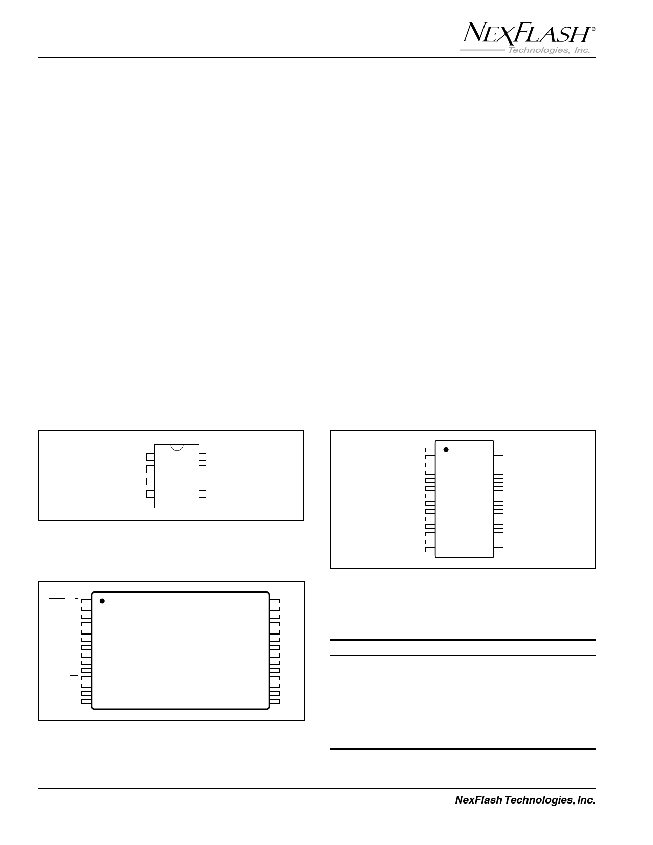
SI
1
SCK 2
Hold R/B 3
CS
4
8
SO
7 GND
6 VCC
5
WP
Figure 3A. NX25F011B and NX25F021B
Pin Assignments, 8-Pin SOIC
HOLD-R/B 1
NC 2
WP 3
NC 4
NC 5
VCC 6
GND 7
NC 8
NC 9
NC 10
CS 11
SCK 12
SI 13
SO 14
28
NC
27
NC
26
NC
25
NC
24
NC
23
NC
22
NC
21
NC
20
NC
19
NC
18
NC
17
NC
16
NC
15
NC
Figure 3B. NX25F011B, NX25F021B, and NX25F041B
Pin Assignments, 28-Pin TSOP (Type I)
GND
1
NC
2
NC
3
CS
4
SCK
5
SI
6
SO
7
NC
8
NC
9
NC
10
NC
11
NC
12
NC
13
NC
14
28
VCC
27
NC
26
NC
25
WP
24
NC
23
HOLD-R/B
22
NC
21
NC
20
NC
19
NC
18
NC
17
NC
16
NC
15
NC
Figure 3C. NX25F041B
Pin Assignments, 28-Pin SOIC
Table 1. Pin Descriptions
SI
SO
SCK
CS
WP
Hold, R/B
Vcc
Serial Data Input
Serial Data Output
Serial Clock Input
Chip Select Input
Write Protect Input
Hold Input or Read Busy Output
Power Supply
6
NexFlash Technologies, Inc.
PRELIMINARY NXSF016F-1201
12/12/01 ©
Share Link: 