L5150GJ 查看數據表(PDF) - STMicroelectronics
零件编号
产品描述 (功能)
生产厂家
L5150GJ Datasheet PDF : 29 Pages
| |||
L5150GJ
3
Application information
Application information
3.1
Voltage regulator
The voltage regulator uses a p-channel mos transistor as a regulating element. With this
structure a very low dropout voltage at current up to 150 mA is obtained. The output voltage
is regulated up to input supply voltage of 40 V. The high-precision of the output voltage (2%)
is obtained with a pre-trimmed reference voltage. The voltage regulator automatically
adapts its own quiescent current to the output current level. In light load conditions the
quiescent current goes down to 55 µA only (low consumption mode). This procedure
features a certain hysteresis on the output current (see Figure 8). Short-circuit protection to
GND and a thermal shutdown are provided.
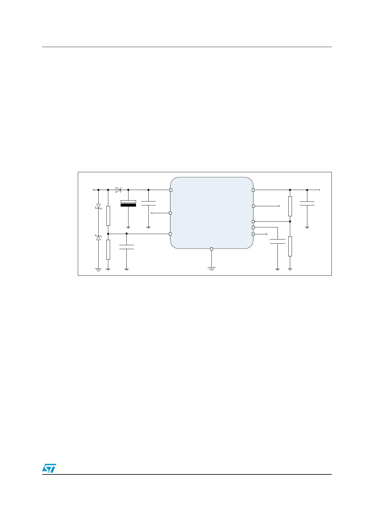
Figure 24. Application schematic
9%$77
9V
&
5(:
5(:
&
(Q
(:L
/*-
*1'
9R
567
5
&R
567B$'-
9FU
(:R
5
*$3*36
The input capacitor C1 ≥ 100 µF is necessary as backup supply for negative pulses which
may occur on the line. The second input capacitor C2 ≥ 220 nF is needed when the C1 is too
distant from the VS pin and it compensates smooth line disturbances. The C0 ceramic
capacitor, connected to the output pin, is for bypassing to GND the high-frequency noise
and it guarantees stability even during sudden line and load variations. Suggested value is
C0 = 220 nF?with ESR ≥ 100 mΩ .
Stability region is reported in Figure 25.
Doc ID 15540 Rev. 12
15/29
Share Link: 