LC5824 查看數據表(PDF) - SANYO -> Panasonic
零件编号
产品描述 (功能)
生产厂家
LC5824 Datasheet PDF : 24 Pages
| |||
LC5824, LC5823, LC5822
EXT-V Specifications
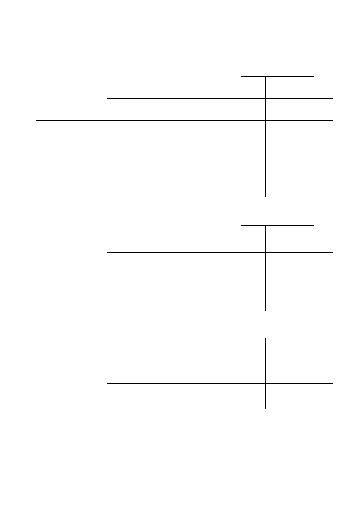
Absolute Maximum Ratings at Ta = 25°C ±2°C, VSS = 0 V
Parameter
Maximum supply voltage
Maximum input voltage
Maximum output voltage
(LCD drive method: 1/3 bias)
(LCD drive methods other than
1/3 bias)
Operating temperature
Storage temperature
Symbol
Conditions and applicable pins
VDD
VDD1
VDD2
VDD3
VDD3
VIN2
VOUT2
VOUT3
VOUT2
Topg
Tstg
(LCD drive method: 1/3 bias)
(LCD drive methods other than 1/3 bias)
S1 to S4, K1 to K4, M1 to M4, A1 to A4, SO1 to SO4,
(With M1 to M4, A1 to A4, and SO1 to SO4 in input mode)
RES, TST
M1 to M4, A1 to A4, SO1 to SO4,
(With M1 to M4, A1 to A4, and SO1 to SO4 in output mode)
ALM, CUP2
SEGOUT, COM1 to COM4, CUP1
M1 to M4, A1 to A4, SO1 to SO4,
(With M1 to M4, A1 to A4, and SO1 to SO4 in output mode)
ALM, SEGOUT, COM1 to COM4, CUP1
min
–0.3
–0.3
–0.3
–0.3
–0.3
–0.3
–0.3
–0.3
–0.3
–20
–30
Ratings
typ
Unit
max
+4.0 V
+4.0 V
+4.0 V
+5.5 V
+4.0 V
VDD + 0.3 V
VDD + 0.3 V
VDD3 + 0.3 V
VDD + 0.3 V
+65 °C
+125 °C
Allowable Operating Ranges at Ta = 25°C ±2°C, VSS = 0 V
Parameter
Supply voltage
High-level input voltage
Low-level input voltage
Operating frequency
Symbol
VDD1
VDD
VDD2
VDD3
VDD3
VIH
VIL
fopg
Conditions and applicable pins
min
1.3
2.0
(LCD drive method: 1/3-bias)
3.9
(LCD drive methods other than 1/3 bias)
VDD3 = VDD2
S1 to S4, K1 to K4, M1 to M4, A1 to A4, SO1 to SO4,
(With M1 to M4, A1 to A4, and SO1 to SO4 in input mode) VDD – 0.4
RES
S1 to S4, K1 to K4, M1 to M4, A1 to A4, SO1 to SO4,
(With M1 to M4, A1 to A4, and SO1 to SO4 in input mode)
0
RES
Ta = –20 + 65°C
32
Ratings
typ
Unit
max
3.6
V
3.6
V
5.0
V
V
VDD
V
0.4
V
33 kHz
Electrical Characteristics at Ta = 25°C ±2°C, VSS = 0 V, VDD = VDD2
Parameter
Input resistance
Symbol
Conditions and applicable pins
RIN1A
RIN1B
RIN2A
RIN2B
RIN3
VDD = 3.0 V, VIN = 0.35 VDD, Low level hold transistor *1,
Figure 5
VDD = 3.0 V, VIN = 0.7 VDD, Programmable pull-down
resistor *1, Figure 5
VDD = 3.0 V, VIN = 0.35 VDD, Input mode, Low level hold
transistor *1, Figure 5
VDD = 3.0 V, VIN = 0.7 VDD, input mode,
Programmable pull-down resistor *2, Figure 5
VDD = 3.0 V, VIN = 0.7 VDD/0.3 VDD
RES pin pull-up/pull-down resistor
Ratings
min
typ
50
Unit
max
500
kΩ
50
1000
kΩ
50
500
kΩ
50
1000
kΩ
10
300
kΩ
Continued on next page.
No. 5944-19/24
Share Link: 