OP06 查看數據表(PDF) - Analog Devices
零件编号
产品描述 (功能)
生产厂家
OP06 Datasheet PDF : 8 Pages
| |||
- ANALOGDEVICES fAX-ON-DEMAND HOTLINE
Page 12
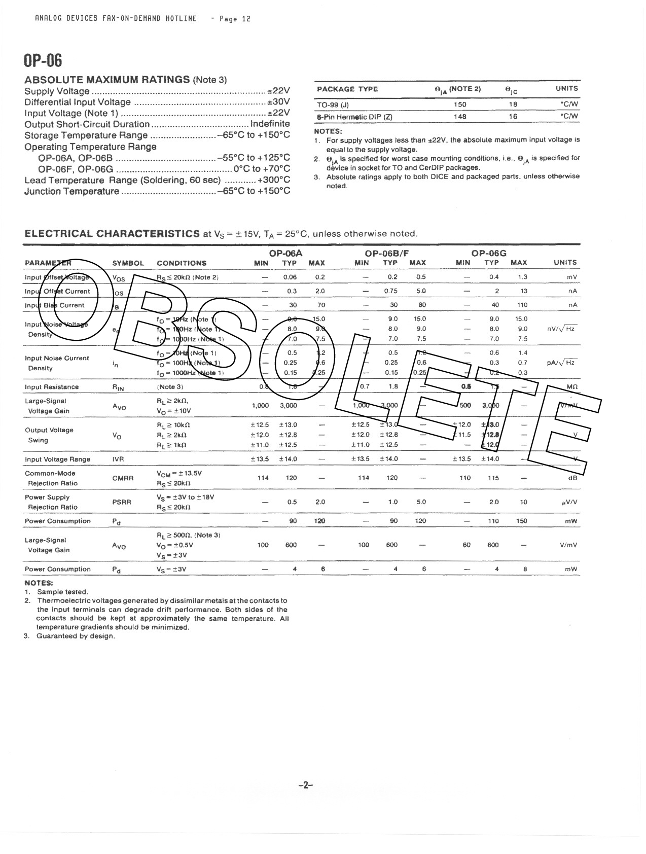
OP-O6
ABSOLUTE MAXIMUM RATINGS (Note 3)
Supply Voltage
:22V
Ditferentiallnput Voltage
:30V
Input Voltage (Note 1)
%22V
Output Short-Circuit Duration
Indefinite
Storage Temperature Range
65°C to +150"C
Operating Temperature Range
OP-O6A, OP-06B
-55°C to +125°C
OP-O6F, OP-O6G
O.C to +70°C
Lead Temperature Range (Soldering, 60 sec) """"""
+300°C
Junction Temperature
65"C to +150°C
PACKAGE TYPE
TO-99 (J)
8-Pin Hermetic DIP (Z)
alA (NOTE 2)
alC
150
18
148
16
UNITS
.C/W
.C/'N
NOTES:
1. For supply voltages less than :22V, the absolute maximum input yoltage is
equal 10the supply voltage.
2. elA is specified for worst case mounting conditions, i.e.. e'A is specified tOf
device in socket for TO and CerOIP packages.
}
3. Absolute ratings apply to both DICE and packaged parts. unless otherwise
noted.
ELECTRICAL CHARACTERISTICS at Vs= :t 15V, TA= 25°C, unless otherwise noted.
OBSO- LETE PARAMETER
Input OffsetVoltage
Input OffsetCurrent
Input BiasCurrent
Input NoiseVoltage
Density
Input NoiseCurrent
Density
Input Resistance
Large-Signal
Voltage Gain
Output Voltage
Swing
SYMBOL
Vos
105
Ie
en
in
R'N
AyO
Vo
CONDITIONS
RSS 2Oktl(Note2;
fo=10Hz(Note1)
fo =tooHz(Note 1)
fO= 1000Hz (Note 1)
fo= 10tU(Note 11
fO= 100Hz (Nota 1)
fo = 1000Hz(No" 1!
(Note 31
RLG:2ktl,
Vo=:!:10V
RL 10ka
RL2kn
AL lkn
OP-06A
MIN TYP
- 0.06
- 0.3
MAX
0.2
2.0
-
30
10
- 9.0 15.0
-
8.0 9.0
- 1.0 1.5
-
0.5 1.2
-
0.25 0.6
0.15 0.25
0.8 1.8 -
1,000 3,000
-
:t12.5 :1:13.0
-
:1:12.0 ;!:12.6
-
:!:1'.0 :!:12.5
-
OP-O6B/F
MIN TYP MAX
-
0.2 0.5
- 0.15 5.0
30
80
9.0 15.0
-
8.0 9.0
-
7.0 7.5
-
0.5 1.2
- 0.25 0.6
- 0.15 0.25
0.1 1.8 -
- 1,000 3,000
:t12.5 :t 13.0 -
:1:12.0 :t12.8
-
:1:11.0 :1:12.5
-
OP-O6G
MIN TYP MAX
-
0.4 1.3
-
2 13
-
40 110
-
9.0 15.0
-
6.0 9.0
-
7.0 7.5
-
0.6 t.4
- 0.3 0.7
-
0.2 0,3
0.5 1.5 -
500 3,000 -
:t 12.0 :1:1"-0
:t 11.5 :1:12.8 -
- :1:12.0 -
UN- ITS
mV
nA
nA
nVI-/Hz
plV-/Hz
IAn
V/mV
V
InputVoltageRange
IVR
:t 13.5 :!:14.0 -
:!:13.S :!:14.0 -
:!:13.5 :t14.0 -
V
Common-Mode
Rejection Ratio
CMRR
VCM =:t 13.5V
Rs:S 2Okn
114
120
-
114
120
-
110
1t5
-
dB
Power Supply
RejectionRatio
Power Consumption
PSRR
Po
Vs=:!:3Vto:!:18V
RSS 2Okfi
- 0,5 2.0
...
-
90 120
- 1.0 5.0
-
90 120
-
2,0 10
-
110 150
IlVN
mW
Large-Signal
VoltageGain
AyO
PowerConsumption Po
Rt 5OOtl. (Note 3i
Vo = :to.5V
Vs =:t3V
Vs =;!:3V
100 600
-
-
4
6
HOTES:
1. Sample tested.
2. Thermoelectric voltages generated by dissimilar metals at the contacts to
the Input terminals can degrade drift performance. Both sides of the
contacts should be kept at approximately the same temperature. All
temperature gradients should be minimized.
3. Guaranteed by design.
100 600
-
-
4
6
60 600 -
-
4
8
V/mV
mW
-2-
~-
-~
----
Share Link: 