BR93LL46F 查看數據表(PDF) - ROHM Semiconductor
零件编号
产品描述 (功能)
生产厂家
BR93LL46F Datasheet PDF : 11 Pages
| |||
Memory ICs
BR93LL46F / BR93LL46FV
(2) Reading
CS
(∗1)
SK
12
4
DI
1 1 0 A5 A4
DO
High-Z
9 10
A1 A0
0 D15 D14
25 26
(∗2)
D1 D0 D15 D14
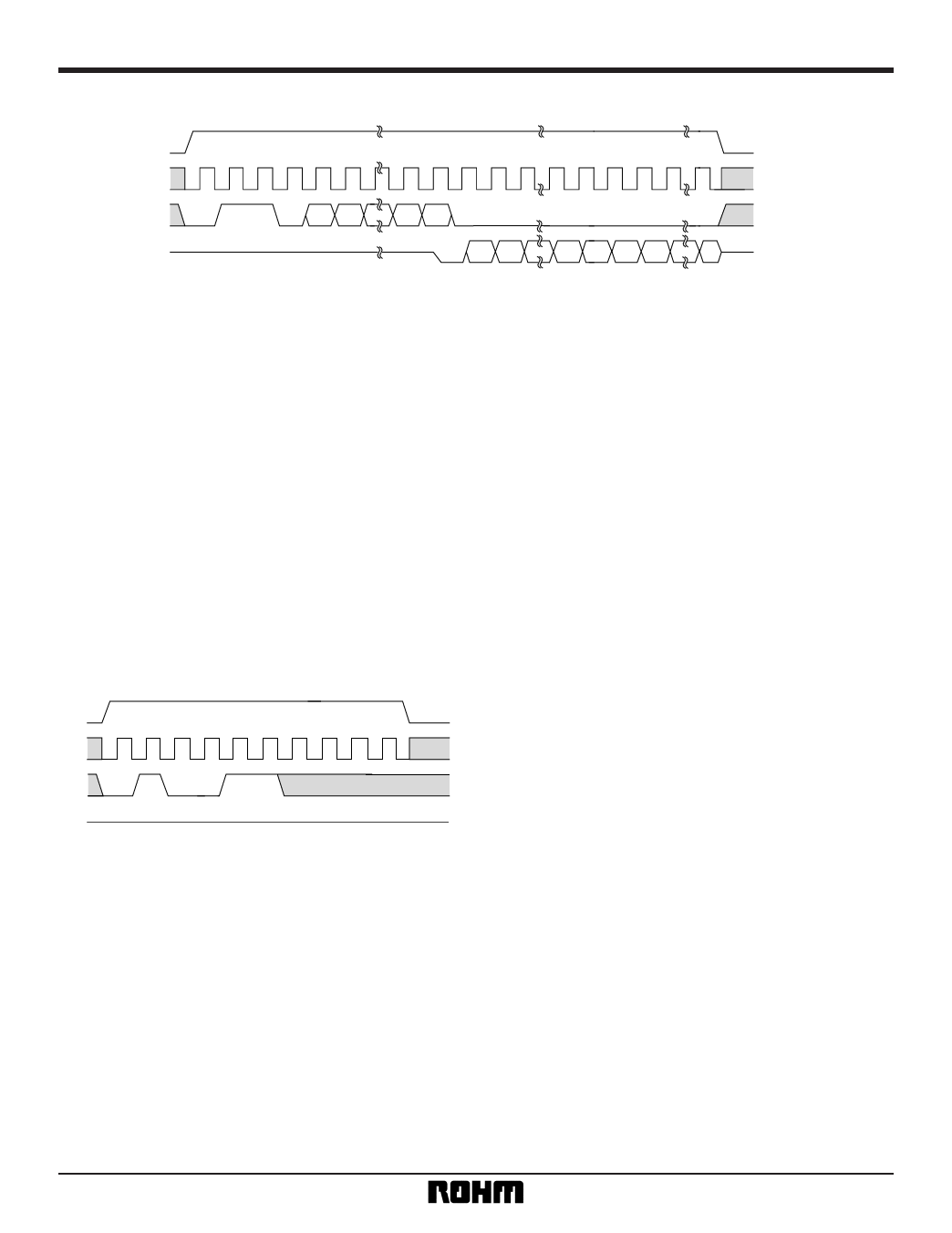
Fig.2 Read cycle timing (READ)
When the read command is acknowledged, the data
(16 bits) for the input address is output serially. The
data is synchronized with the SK rise during A0 acqui-
sition and a “0” (dummy bit) is output. All further data is
output in synchronization with the SK pulse rises.
( ∗1) Start bit
The start bit is taken as the first “1” that is received
after the CS pin rises. Also, if “0” is input several times
followed by “1”, the “1” is recognized as a start bit, and
subsequent operation commences.
This applies also to the following commands.
( ∗2) Address auto increment function
These ICs are equipped with an address auto incre-
ment function which is effective only during reading
operations. With this function, if the SK clock is input
following execution of one of the above reading com-
mands, data is read from upper addresses in succes-
sion. CS is held in HIGH state during automatic incre-
menting.
(3) Write enable
CS
SK
DI
1 0 01 1
DO
High-Z
Fig.3 Cycle timing that allows overwriting
These ICs are set to the write disabled state by the
internal reset circuit when the power is turned on.
Therefore, before performing a write command, the
write enable command must be executed. When this
command is executed, it remains valid until a write dis-
able command is issued or the power supply is cut off.
However, read commands can be used in either the
write enable or write disable state.
5
Share Link: 