LH543620P-25 жҹҘзңӢж•ёж“ҡиЎЁпјҲPDFпјү - Sharp Electronics
йӣ¶д»¶зј–еҸ·
дә§е“ҒжҸҸиҝ° (еҠҹиғҪ)
з”ҹдә§еҺӮ家
LH543620P-25 Datasheet PDF : 38 Pages
| |||
1024 Г— 36 Synchronous FIFO
LH543620
PIN NAME
DESCRIPTION
FF
AF
HF
MFF
STATUS FLAGS SYNCHRONOUS TO THE INPUT CLOCK
Full Flag. FF is synchronous to the rising edge of CKI. When asserted LOW, 1024 36-bit words of
the FIFO memory array contain meaningful data. When FF is asserted, writing data to the FIFO is
disabled.
Almost-Full Flag. When asserted LOW, AF indicates that there are at most вҖҳpвҖҷ vacant 36-bit
words remaining in the FIFO memory array, where вҖҳpвҖҷ is the value of the Almost-Full-Offset-Value.
AF has two synchronization modes depending on Bit 5 of the control register.
Bit 5 = 0 (Default) Asynchronous Mode
Bit 5 = 1: AF is synchronous to the rising edge of CKI.
Half-Full Flag. When asserted LOW, there are at least 513 36-bit words in the FIFO memory
array. HF has three synchronization modes depending on Bits 3 and 4 of the control register. See
Table 3.
Mailbox-Full Flag. MFF is synchronized to the rising edge of CKI. When asserted LOW, it
indicates that a new mail word has been placed in the mailbox.
CONTROL SIGNALS SYNCHRONOUS TO THE OUTPUT CLOCK
Output-Port Enables. ENO1 and ENO2 are active HIGH, synchronous to the rising edge of CKO.
ENO1, ENO2 Data is read from the FIFO memory array when both ENO1, ENO2 are asserted.
NOTE: ENO1, ENO2 DO NOT ENABLE reading data from the Resource Register or the Mailbox.
ADO[2:0]
Output-Port Address. ADO[2:0] specifies the Output-Port source/destination. See Table 4.
ADO[2:0] is synchronous to the rising edge of CKO.
NOTE: In order to read the resource register at the output bus, BYE should be deasserted and the
FIFO memory array should be disabled.
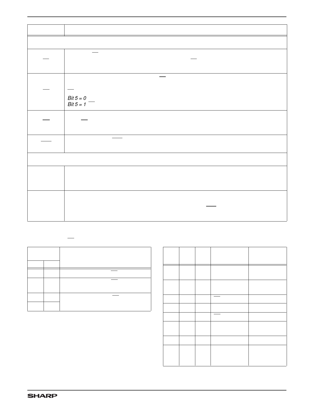
Table 3. HF Synchronization Modes
CONTROL
REGISTER
BIT 4 BIT 3
FUNCTION
L * L * Asynchronous Mode: HF
L
H
Synchronous Mode I: HF is
synchronous to the rising edge of CKO
H L Synchronous Mode II: HF is
H H synchronous to the rising edge of CKI
* Default Mode
Table 4. Output-Port Address
ADO2 ADO1 ADO0
SELECTION
DEFAULT VALUE
(of the selected
REGISTER)
L
L
L
RBASE
register
0
L
L
H
ROFFSET
register
0
L H L AF offset value
8
L H H Parity register
0
H L L AE offset value
8
H
L
H
Control
register
1
H H L Mailbox
0
Resource
H H H registers read Not applicable
disabled
11
Share Link: 