A28F010 查看數據表(PDF) - Intel
零件编号
产品描述 (功能)
生产厂家
A28F010 Datasheet PDF : 23 Pages
| |||
A28F010
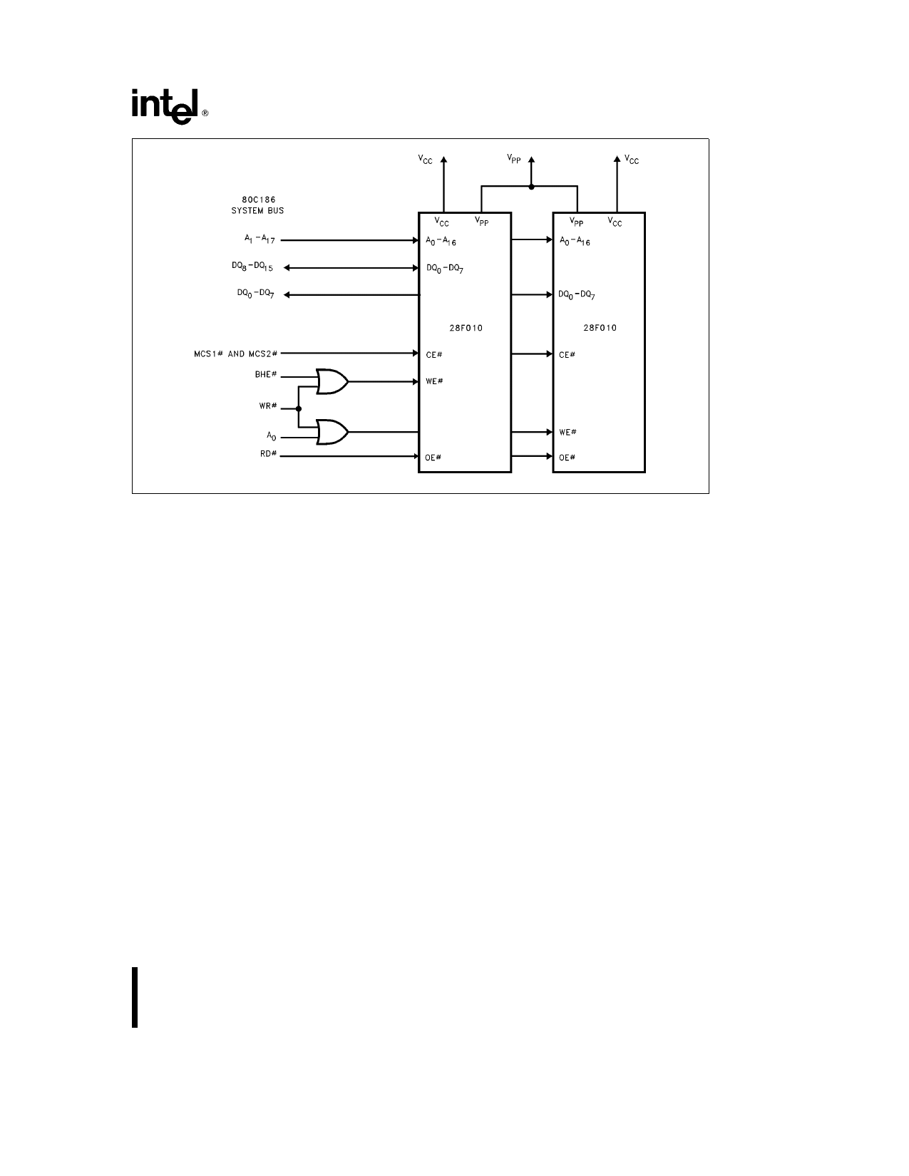
Figure 3 28F010 in a 80C186 System
290266 – 4
PRINCIPLES OF OPERATION
Flash-memory augments EPROM functionality with
in-circuit electrical erasure and reprogramming The
28F010 introduces a command register to manage
this new functionality The command register allows
for 100% TTL-level control inputs fixed power sup-
plies during erasure and programming and maxi-
mum EPROM compatibility
In the absence of high voltage on the VPP pin the
28F010 is a read-only memory Manipulation of the
external memory-control pins yields the standard
EPROM read standby output disable and Intelli-
gent Identifier operations
The same EPROM read standby and output disable
operations are available when high voltage is ap-
plied to the VPP pin In addition high voltage on VPP
enables erasure and programming of the device All
functions associated with altering memory con-
tents Intelligent Identifier erase erase verify pro-
gram and program verify are accessed via the
command register
Commands are written to the register using standard
microprocessor write timings Register contents
serve as input to an internal state-machine which
controls the erase and programming circuitry Write
cycles also internally latch addresses and data
needed for programming or erase operations With
the appropriate command written to the register
standard microprocessor read timings output array
data access the Intelligent Identifier codes or out-
put data for erase and program verification
Integrated Program Erase Stop Timer
Successive command write cycles define the dura-
tions of program and erase operations specifically
the program or erase time durations are normally
terminated by associated program or erase verify
commands An integrated stop timer provides simpli-
fied timing control over these operations thus elimi-
nating the need for maximum program erase timing
specifications Program and erase pulse durations
are minimums only When the stop timer terminates
a program or erase operation the device enters an
inactive state and remains inactive until receiving the
appropriate verify or reset command
Write Protection
The command register is only alterable when VPP is
at high voltage Depending upon the application the
system designer may choose to make the VPP pow-
er supply switchable available only when memory
updates are desired When high voltage is removed
5
Share Link: 