NTE7016 查看數據表(PDF) - NTE Electronics
零件编号
产品描述 (功能)
生产厂家
NTE7016 Datasheet PDF : 3 Pages
| |||
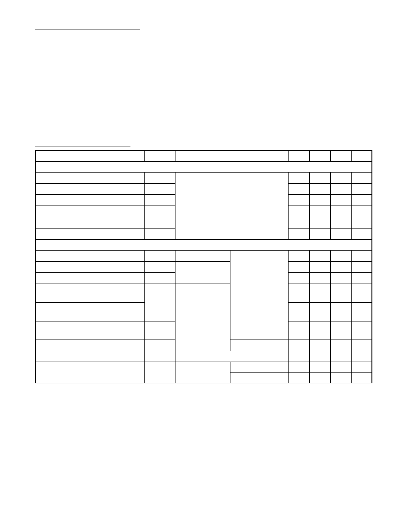
Absolute Maximum Ratings: (TA = +25°C unless otherwise specified)
DC Supply Voltage (Between Pin11 and Pin4) . . . . . . . . . . . . . . . . . . . . . . . . . . . . . . . . . . . . . . . . 16V
(Between Pin11 and Pin14) . . . . . . . . . . . . . . . . . . . . . . . . . . . . . . . . . . . . . . . 16V
DC Current (Out of Pin15) . . . . . . . . . . . . . . . . . . . . . . . . . . . . . . . . . . . . . . . . . . . . . . . . . . . . . . . . . . 2mA
Device Dissipation, PD
Up to TA = +85°C . . . . . . . . . . . . . . . . . . . . . . . . . . . . . . . . . . . . . . . . . . . . . . . . . . . . . . . . . 640mW
Derate linearly above TA = +85°C . . . . . . . . . . . . . . . . . . . . . . . . . . . . . . . . . . . . . . . . 9.9mW/°C
Operating Ambient Temperature Range, Topr . . . . . . . . . . . . . . . . . . . . . . . . . . . . . . . . . . –40° to +85°C
Storage Temperature Range, Tstg . . . . . . . . . . . . . . . . . . . . . . . . . . . . . . . . . . . . . . . . . . –65° to +150°C
Lead Temperature (During Soldering), TL
(At a distance not less than 1/32” (0.79mm) from case for 10sec max) . . . . . . . . . . . +265°C
Electrical Characteristics: (TA = +25°C, V+ = 12V unless otherwise specified)
Parameter
Symbol
Test Conditions
Min Typ Max Unit
Static (DC) Characteristics
Quiescent Circuit Current
I11
IF Input (Pin1)
V1
20 31 40 mA
1.2 1.9 2.4 V
AC Return to Input (Pin2)
DC Bias to Input (Pin3)
V2
No Signal Input, Non Muted
V3
1.2 1.9 2.4 V
1.2 1.9 2.4 V
RF AGC (Pin15)
V15
DC Reference (Pin10)
V10
7.5 9.5 11.0 V
5.0 5.6 6.0 V
Dynamic Characteristics
Input Limiting Voltage (–3dB Point) VI(lim)
– 12 25 µV
AM Rejection (Pin6)
Recovered AF Voltage (Pin6)
AMR VIN = 0.1V,
VO(AF) AM Mod. = 30%
45 55 – dB
325 500 650 mV
Total Harmonic Distortion:
Single Tuned (Pin6) Note 1
Total Harmonic Distortion:
THD
fO = 10.7MHz,
– 0.5 1.0 %
fmod = 400Hz,
Deviation ±75kHz – 0.1 – %
Double Tuned (Pin6) Note 1
VIN = 0.1V
Signal Plus Noise to Noise Ratio S + N/N
65 72 – dB
(Pin6)
Deviation Mute Frequency
fDEV
fmod = 0
– ±40 – kHz
RF AGC Threshold
ON Channel Step
V16
V12 VIN = 0.1V
fDEV < ±40kHz
fDEV > ±40kHz
– 1.25 – V
–0–V
– 5.6 – V
Note 1. THD characteristics are essentially a function of the phase characteristics of the network
connected between Pin8, Pin9, and Pin10.
Share Link: 