MAX6467(2002) 查看數據表(PDF) - Maxim Integrated
零件编号
产品描述 (功能)
生产厂家
MAX6467
(Rev.:2002)
(Rev.:2002)
Maxim Integrated

MAX6467 Datasheet PDF : 9 Pages
| |||
Microprocessor Supervisory Reset Circuits
with Edge-Triggered, One-Shot Manual Reset
ABSOLUTE MAXIMUM RATINGS
VCC to GND ...........................................................-0.3V to +6.0V
RESET to GND
Open-Drain........................................................-0.3V to +6.0V
Push-Pull.................................................-0.3V to (VCC + 0.3V)
MR to GND .................................................-0.3V to (VCC + 0.3V)
Input/Output Current (all pins) ............................................20mA
Continuous Power Dissipation (TA = +70°C)
4-Pin SC70 (derate 3.1mW/°C above +70°C) ..............245mW
4-Pin SOT143 (derate 4mW/°C above +70°C).............320mW
Operating Temperature Range .........................-40°C to +125°C
Storage Temperature Range .............................-65°C to +150°C
Junction Temperature ......................................................+150°C
Lead Temperature (soldering, 10s) .................................+300°C
Stresses beyond those listed under “Absolute Maximum Ratings” may cause permanent damage to the device. These are stress ratings only, and functional
operation of the device at these or any other conditions beyond those indicated in the operational sections of the specifications is not implied. Exposure to
absolute maximum rating conditions for extended periods may affect device reliability.
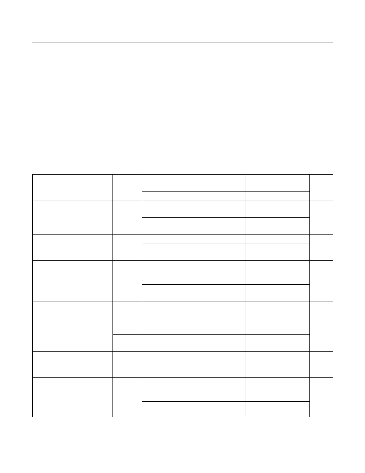
ELECTRICAL CHARACTERISTICS
(VCC = +1.2V to +5.5V, TA = -40°C to +125°C, unless otherwise noted. Typical values are at TA = +25°C.) (Note 1)
PARAMETER
Operating Voltage Range
Supply Current
VCC Reset Threshold
(See the Reset Threshold Table)
VCC Reset Delay
VCC Reset Timeout Period
MR Timeout Period
MR Rising Debounce Period
(Note 2)
MR Input Voltage
MR Minimum Input Pulse
MR Glitch Rejection
MR to RESET Delay
MR Pullup Resistance
RESET Output High
(MAX6468 Only)
SYMBOL
VCC
ICC
VTH
tRD
tRP
tMRP
CONDITIONS
TA = 0°C to +125°C
TA = -40°C to 0°C
VCC = +5.5V, no load
VCC = +3.6V, no load
VCC = +2.5V, no load
VCC = +1.8V, no load
TA = +25°C
TA = -40°C to +85°C
TA = +85°C to +125°C
VCC falling at 10mV/µs from VTH + 100mV
to VTH - 100mV
D3 option
D7 option
D3 and D7 options
MIN
1.0
1.2
-1.5%
-2.5%
-3%
150
1200
150
TYP MAX UNITS
5.5
V
5.5
7
13
6
11
µA
4
8
3
7.5
VTH +1.5%
+2.5%
V
+3%
35
µs
225 300
ms
1800 2400
225 300
ms
tDEB D3 and D7 options
150
225
300
ms
VIL
VIH
VTH < +4V
VIL
VIH
VTH ≥ +4V
0.7 x VCC
2.4
0.3 x VCC
V
0.8
1
µs
100
ns
200
ns
MR to VCC
750 1500 2250
Ω
VCC ≥ +2.5V, ISOURCE = 500µA, RESET not
asserted
0.8 x VCC
VOH
V
VCC ≥ +4.5V, ISOURCE = 800µA, RESET not
asserted
0.8 x VCC
2 _______________________________________________________________________________________
Share Link: