MAX6467US17D3-T(2015) 查看數據表(PDF) - Maxim Integrated
零件编号
产品描述 (功能)
生产厂家
MAX6467US17D3-T
(Rev.:2015)
(Rev.:2015)
Maxim Integrated

MAX6467US17D3-T Datasheet PDF : 10 Pages
| |||
MAX6467/MAX6468
Microprocessor Supervisory Reset Circuits
with Edge-Triggered, One-Shot Manual Reset
Reset Timeout Delay*
RESET TIMEOUT SUFFIX
D3
VCC RESET TIMEOUT PERIOD
(min/max) (ms)
150/300
MR TIMEOUT PERIOD
(min/max) (ms)
150/300
D7
1200/2400
150/300
*Additional reset timeout options may be available. Contact factory for availability.
MR RISING DEBOUNCE PERIOD
(min/max) (ms)
150/300
150/300
Applications Information
Falling VCC Transients
In addition to issuing a reset to the µP during power-up,
power-down, and brownout conditions, the MAX6467/
MAX6468 are relatively immune to short-duration fall-
ing VCC transients (glitches). The Typical Operating
Characteristics section shows the Maximum Transient
Duration vs. VCC Overdrive for which the MAX6467/
MAX6468 do not generate a reset pulse. This graph was
generated using a falling pulse applied to VCC starting
above the actual reset threshold and ending below the
threshold by the magnitude indicated (VCC Overdrive).
The graph indicates the typical maximum pulse width a
falling VCC transient can have without initiating a reset
pulse. As the magnitude of the transient increases (goes
farther below the reset threshold), the maximum allowable
pulse width decreases. A 0.1µF bypass capacitor from
VCC to GND provides additional transient immunity.
Ensuring a Valid RESET Output Down
to VCC = 0V
The MAX6467/MAX6468 guarantee proper operation
down to VCC = +1V. In applications that require valid
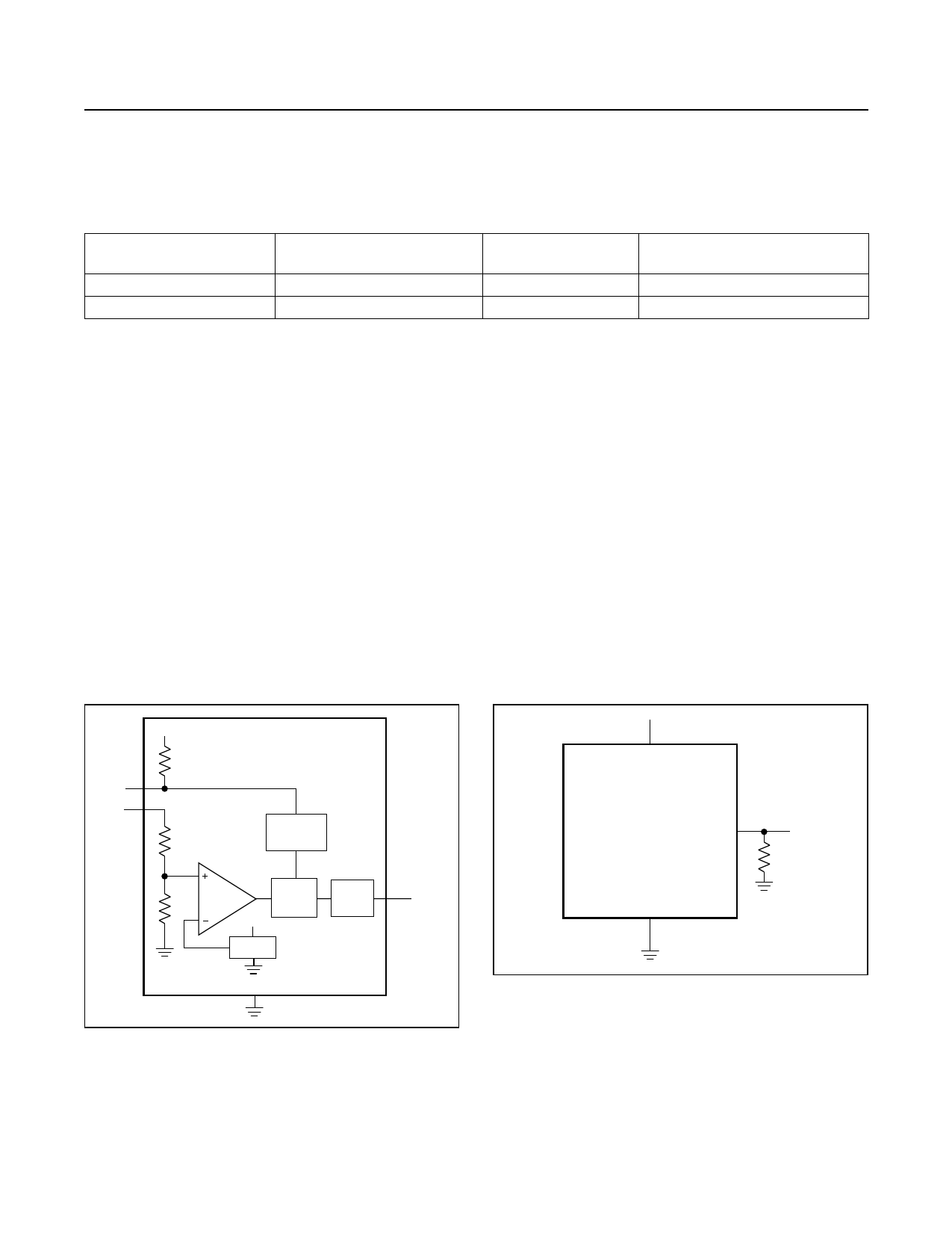
reset levels down to VCC = 0V, a pulldown resistor to
active-low outputs (MAX6468 only, Figure 3) ensures
that RESET remains valid while the RESET output can
no longer sink current. This scheme does not work with
the open-drain outputs of the MAX6467. Ensure that the
resistor value used does not overload the RESET output
when VCC is above the reset threshold. For most applica-
tions, use 100kΩ to 1MΩ.
VCC
1.5kΩ
MR
VCC
MAX6467
MAX6468
MR ONE-SHOT/
DEBOUNCE
RESET
TIMEOUT
PERIOD
VCC
1.23V
RESET
OUTPUT
RESET
GND
Figure 2. Functional Diagram
VCC
MAX6468
RESET
R1
100kΩ
GND
Figure 3. RESET Valid to VCC = 0V
Chip Information
TRANSISTOR COUNT: 748
PROCESS: BiCMOS
www.maximintegrated.com
Maxim Integrated │ 7
Share Link: