AU5783D 查看數據表(PDF) - Philips Electronics
零件编号
产品描述 (功能)
生产厂家
AU5783D Datasheet PDF : 14 Pages
| |||
Philips Semiconductors
J1850/VPW transceiver with supply control function
Objective specification
AU5783
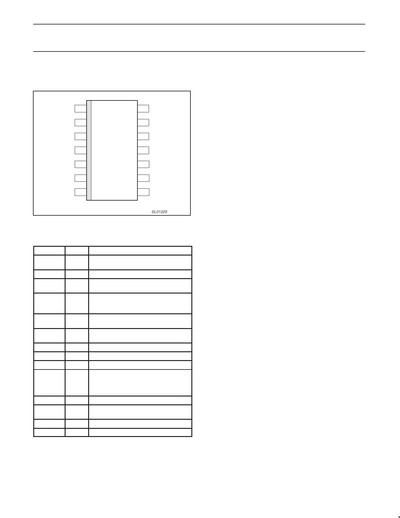
PINNING
Pin configuration
R/F 1
GND 2
4X/LOOP 3
NSTB 4
TX 5
RX 6
N.C. 7
14 GND
13 N.C.
12 BUS
AU5783
11 LOAD
10 INH
9
LWAKE
8
BAT
SO14
SL01225
Figure 2. Pin configuration
Pin description
SYMBOL PIN
R/F
1
GND
2
4X/LOOP
3
NSTB
4
TX
5
RX
6
N.C.
7
BAT
8
LWAKE
9
INH
10
LOAD
11
BUS
12
N.C.
13
GND
14
DESCRIPTION
Rise/fall time control input; connect to
ground potential via a resistor
Ground
Tx mode control input; low: normal mode;
high: 4X mode; float: loopback
Network STandBy power control input;
low: transmit function disabled (low power
modes); high: transmit function enabled
Transmit data input; low: transmitter
passive; high: transmitter active
Receive data output; low: active bus
condition detected; high: otherwise
Not connected
Battery supply input, 12V nominal
Local wake-up input, edge sensitive
Activity indication flag (inhibit) output high
side driver; e.g., to control a voltage
regulator. Active high enables the
regulator
Bus load in/output
Bus line transmit/receive input/output,
active high side driver
Not connected
Ground
FUNCTIONAL DESCRIPTION
The AU5783 is an integrated line transceiver IC that interfaces an
SAE/J1850 protocol controller IC to the vehicle’s multiplex bus line.
It is primarily intended for automotive “Class B” multiplexing
applications in passenger cars using VPW (Variable Pulse Width)
modulated signals with a nominal transmission speed of 10.4 kbit/s.
The device provides transmit and receive capability as well as
protection to a J1850 electronic module.
A J1850 link controller feeds the transmit data stream to the
transceiver’s TX input. The AU5783 transceiver waveshapes the TX
data input signal so as to minimize electromagnetic emission. The
bus output signal features controlled rise & fall characteristic
including rounded shape. A resistance being connected to the R/F
control input sets the bus output slew rate.
The LOAD output is connected to the physical bus line via an
external load resistor Rld. The load resistor pulls the bus line to
ground potential being the default state e.g. when no transmitter
outputs an active state. This output ensures the J1850 network will
not be affected by a potential loss of ground condition at an
individual electronic control unit.
The AU5783 includes a bus receiver with filter function to minimize
susceptibility against interference. The logic state of the J1850 bus
signal is indicated at the RX output being connected to the J1850
link controller.
The AU5783 also provides advanced low-power modes to help
minimize ignition-off power consumption of an electronic control unit.
The bus receiver function is kept alive in the low-power modes. If an
active state is being detected on the bus line this will be indicated
via the RX output. By default the AU5783 enters the low-power
standby mode when the mode control inputs NSTB and 4X/LOOP
are not driven.
Ignition-off current draw can be reduced further by turning off the
voltage regulator being typically provided in an electronic control
unit. This is supported by the activity indication function of the
AU5783. In this application the activity indication flag INH will control
external devices such as a voltage regulator. To turn-off the INH flag
and thus the voltage regulator, the go to sleep command needs to
be applied to the Network Standby power control input,
e.g., NSTB = 0. The INH output is turned off after the sleep time-out
period thereby, reducing the power consumption of an electronic
control unit to an extremely low level.
The activity indication flag INH will be turned on again upon
detection of a remote wake-up condition (i.e. bus activity) or upon
detection of a local wake-up condition or a respective command
from the microcontroller. A local wake-up condition is detected when
an edge occurs at the wake-up input LWAKE. The INH flag will also
be turned on upon detection of a high input level at the mode control
input NSTB. Activation of the INH output enables external devices
e.g., a voltage regulator. This condition will power-up logic devices
e.g., a microcontroller in order to perform appropriate action,
e.g., activation of the AU5783 and the J1850 network.
The AU5783 provides a high-speed data transmission mode where
the bus output waveshape function is disabled. In this mode transmit
signals are output as fast as possible thus allowing higher data
rates, e.g. the so-called 4X mode with 41.6 kbit/s nominal speed.
The AU5783 also provides a loop-back mode for diagnostic
purpose, e.g. self-test of an electronic control unit. In loop-back
mode the bus transmit and receive functions are disabled thus
1999 May 11
4
Share Link: 