AU5783D 查看數據表(PDF) - Philips Electronics
零件编号
产品描述 (功能)
生产厂家
AU5783D Datasheet PDF : 14 Pages
| |||
Philips Semiconductors
J1850/VPW transceiver with supply control function
Objective specification
AU5783
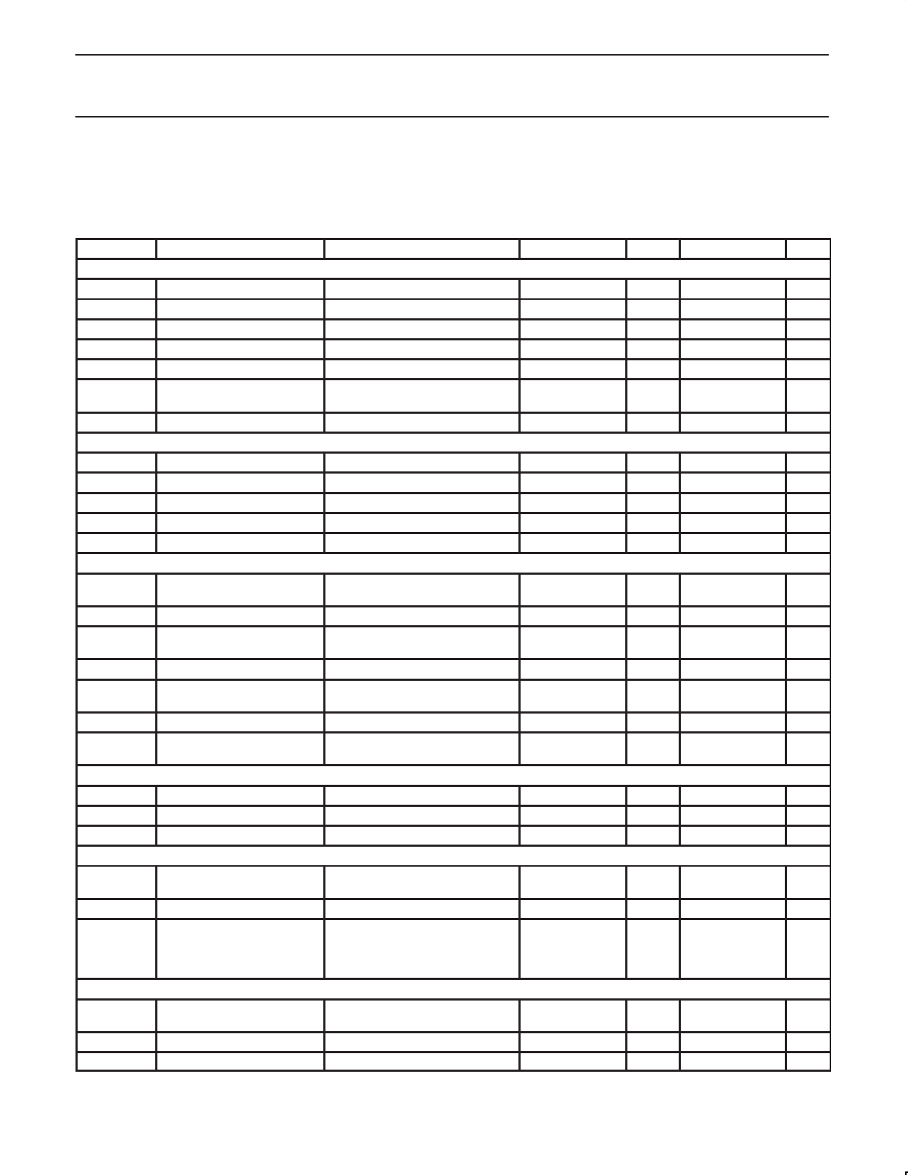
DC ELECTRICAL CHARACTERISTICS
7V < VBAT < 16V; –40 °C < Tamb < +125 °C; 250W < RL < 1.6 kΩ; 1.4 kΩ < Rld < 12 kΩ;
–2V < Vbus < +9V; NSTB = 5V; 4X/LOOP = 5V; Rs = 56 kΩ; RX connected to +5V via Rd = 3.9 kΩ; INH loaded with 100 kΩ to GND;
LWAKE connected to BAT via 10 kΩ resistor; all voltages are referenced to pin 14 (GND); positive currents flow into the IC;
typical values reflect the approximate average value at VBAT = 13V and Tamb = 25 °C; unless otherwise specified.
SYMBOL
PARAMETER
CONDITIONS
MIN.
TYP.
MAX.
Pin BAT & thermal shutdown
IBAT.sl
Sleep mode supply current Note 6
90
IBAT.sb
Standby mode supply current Note 6
210
IBAT.p
Supply current; passive state TX = 0V; LWAKE = 0V
3
IBAT.wl
Supply current; weak load
TX = 5V, RL = 1.38 kΩ, Note 7
16
IBAT.fl
Supply current; full load
TX = 5V, RL = 250Ω
45
Tsd
Thermal shutdown
temperature
Note 7
155
190
Thys
Thermal shutdown hysteresis Note 7
Pins TX, NSTB
5
15
Vih
High level input voltage
2.7
Vil
Low level input voltage
0.9
Iihtx
TX high level input current
VTX = 5V
50
200
Iihnstb
NSTB high level input current VNSTB = 5V
10
50
Iil
Low level input current
Vi = 0V
–2
+2
Pin 4X/LOOP
Vih
High level input voltage (High NSTB = 5V
2.7
Speed Mode)
Iih
High level input current
V4X = 5V, NSTB = 5V
50
200
Vilb
Mid level input voltage (Loop NSTB = 5V
1.3
1.9
back operation)
Iilb
Loopback mode input current NSTB = 5V
–10
Vil
Low level input voltage
NSTB = 5V
(Normal Mode)
+10
+0.7
–Iil
Low level input current
V4X = 0V, NSTB = 5V
50
200
–Iils
Low level input current in
V4X = 0V, NSTB = 0V
–5
+5
standby and sleep mode
Pin LWAKE
Vi_wh
Local wake-up high
NSTB = 0V
3.9
Vi_Wl
Local wake-up low
NSTB = 0V
2.5
–II_w
Low level input current
VLWAKE = 0V
5
25
Pin INH
–Ioh_inh
INH high level output current VINH = VBAT – 1V;
120
500
4.9V < VBAT < 16V
–Iol_inh
INH off-state output leakage VINH = 0V; NSTB = 0V
–5
+5
Vbat_POR Power-on reset release
NSTB = 1V, BUS = 0V,
3.5
4.4
voltage; Battery voltage
VBAT = 3.5V, verify INH = 0;
threshold for setting INH
VBAT = 4.4V, verify INH = 1
output
Pin RX
Vol_rx
Low level output voltage
IRX = 1.6 mA, BUS = 7V,
0
all modes
0.45
Iol_rx
Low level output current
VRX = 5V, BUS = 7V
2
20
Ioh_rx
High level output leakage
VRX = 5V, BUS = 0V, all modes
–10
+10
UNIT
µA
µA
mA
mA
mA
°C
°C
V
V
µA
µA
µA
V
µA
V
µA
V
µA
µA
V
V
µA
µA
µA
V
V
mA
µA
1999 May 11
7
Share Link: 