74VHC125BQ 查看數據表(PDF) - NXP Semiconductors.
零件编号
产品描述 (功能)
生产厂家
74VHC125BQ Datasheet PDF : 15 Pages
| |||
Nexperia
74VHC125; 74VHCT125
Quad buffer/line driver; 3-state
Table 7. Dynamic characteristics …continued
GND = 0 V; For test circuit see Figure 8.
Symbol Parameter Conditions
For type 74VHCT125
tpd
propagation nA to nY; see Figure 6
delay
VCC = 4.5 V to 5.5 V
CL = 15 pF
CL = 50 pF
ten
enable time nOE to nY; see Figure 7
VCC = 4.5 V to 5.5 V
CL = 15 pF
CL = 50 pF
tdis
disable time nOE to nY; see Figure 7
VCC = 4.5 V to 5.5 V
CL = 15 pF
CL = 50 pF
CPD
power
CL = 50 pF; fi = 1 MHz;
dissipation VI = GND to VCC
capacitance
25 °C
−40 °C to +85 °C −40 °C to +125 °C Unit
Min Typ[1] Max Min
Max
Min
Max
[2]
- 3.0 5.5 1.0
6.5
1.0
7.0 ns
- 4.3 7.5 1.0
8.5
1.0
9.5 ns
- 3.4 5.1 1.0
6.0
1.0
6.5 ns
- 4.9 7.3 1.0
8.3
1.0
9.5 ns
[2]
- 4.5 6.8 1.0
8.0
1.0
8.5 ns
- 6.5 8.8 1.0
10.0
1.0
11.0 ns
[3] -
12 -
-
-
-
-
pF
[1] Typical values are measured at nominal supply voltage (VCC = 3.3 V and VCC = 5.0 V).
[2] tpd is the same as tPLH and tPHL.
ten is the same as tPZL and tPZH.
tdis is the same as tPLZ and tPHZ.
[3] CPD is used to determine the dynamic power dissipation (PD in µW).
PD = CPD × VCC2 × fi × N + Σ(CL × VCC2 × fo) where:
fi = input frequency in MHz, fo = output frequency in MHz
CL = output load capacitance in pF
VCC = supply voltage in Volts
N = number of inputs switching
Σ(CL × VCC2 × fo) = sum of the outputs.
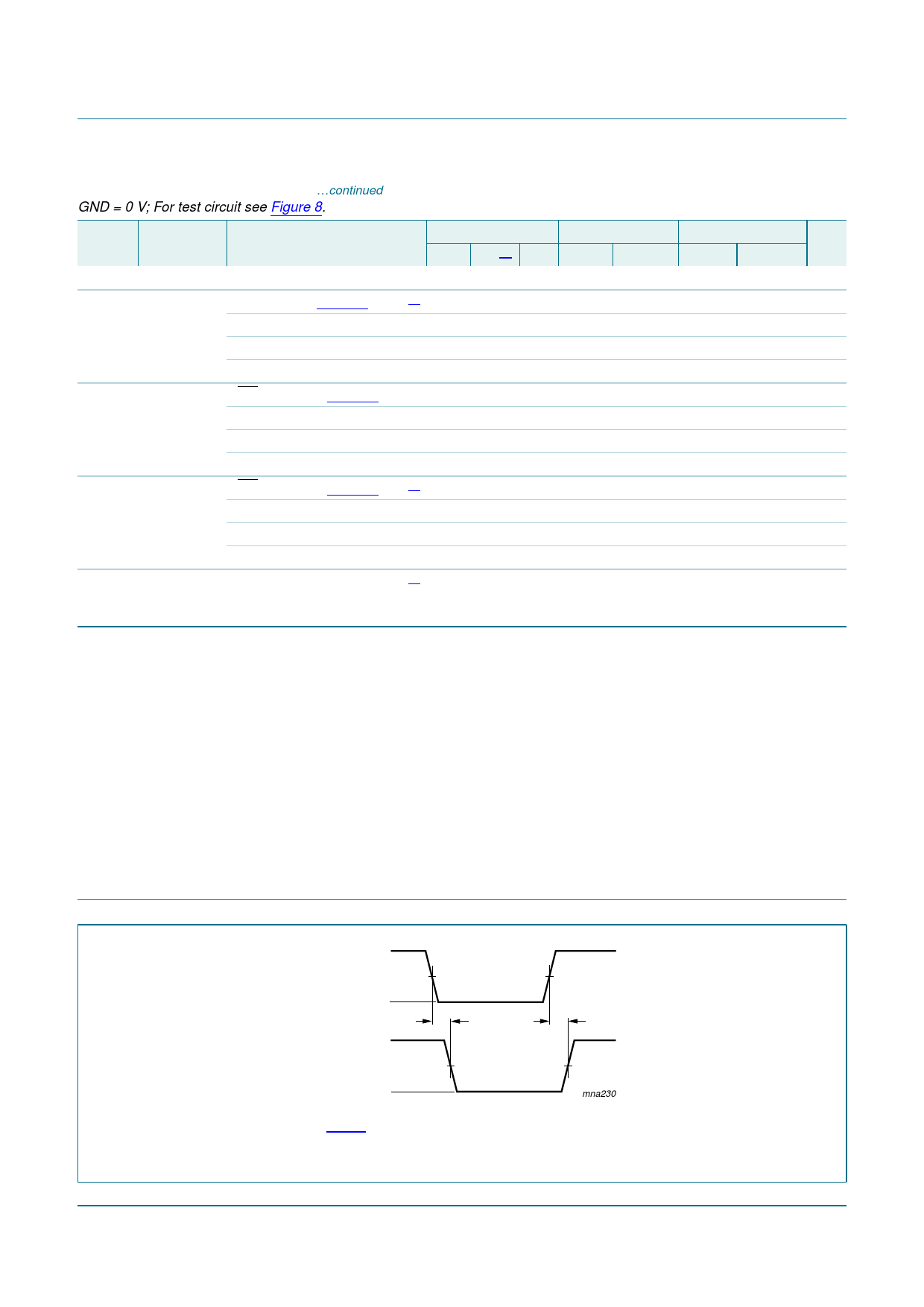
11. Waveforms
VI
nA input
GND
VOH
nY output
VOL
VM
tPHL
VM
tPLH
mna230
Fig 6.
Measurement points are given in Table 8.
VOL and VOH are typical voltage output levels that occur with the output load.
Propagation delay input (nA) to output (nY)
74VHC_VHCT125_2
Product data sheet
Rev. 02 — 13 October 2009
© Nexperia B.V. 2017. All rights reserved
7 of 15
Share Link: 