AD9204(RevA) 查看數據表(PDF) - Analog Devices
零件编号
产品描述 (功能)
生产厂家
AD9204
(Rev.:RevA)
(Rev.:RevA)
Analog Devices

AD9204 Datasheet PDF : 36 Pages
| |||
AD9204
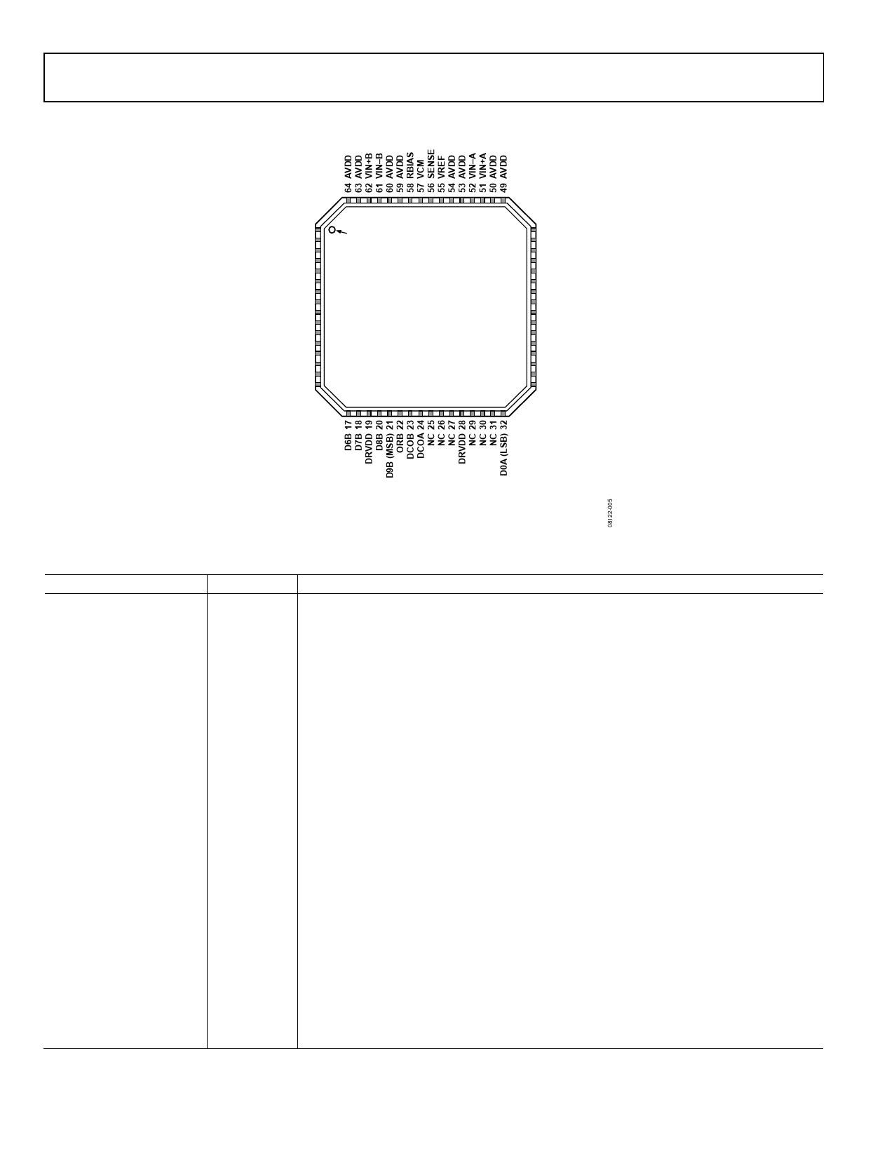
PIN CONFIGURATION AND FUNCTION DESCRIPTIONS
Data Sheet
CLK+ 1
CLK– 2
SYNC 3
NC 4
NC 5
NC 6
NC 7
NC 8
NC 9
DRVDD 10
D0B (LSB) 11
D1B 12
D2B 13
D3B 14
D4B 15
D5B 16
PIN 1
INDICATOR
AD9204
TOP VIEW
(Not to Scale)
48 PDWN
47 OEB
46 CSB
45 SCLK/DFS
44 SDIO/DCS
43 ORA
42 D9A (MSB)
41 D8A
40 D7A
39 D6A
38 D5A
37 DRVDD
36 D4A
35 D3A
34 D2A
33 D1A
NOTES
1. NC = NO CONNECT
2. THE EXPOSED PADDLE MUST BE SOLDERED TO THE PCB GROUND
TO ENSURE PROPER HEAT DISSIPATION, NOISE, AND MECHANICAL
STRENGTH BENEFITS.
Figure 5. Pin Configuration
Table 8. Pin Function Description
Pin No.
Mnemonic
0
GND
1, 2
CLK+, CLK−
3
SYNC
4, 5, 6, 7, 8, 9, 25, 26, 27,
NC
29, 30, 31
10, 19, 28, 37
DRVDD
11 to 18, 20, 21
D0B to D9B
22
ORB
23
DCOB
24
DCOA
32 to 36, 38 to 42
D0A to D9A
43
ORA
44
SDIO/DCS
45
SCLK/DFS
46
CSB
47
OEB
48
PDWN
Description
Exposed paddle is the only ground connection for the chip. Must be connected to PCB AGND.
Differential Encode Clock. PECL, LVDS, or 1.8 V CMOS inputs.
Digital Input. SYNC input to clock divider. 30 kΩ internal pull-down.
Do Not Connect.
Digital Output Driver Supply (1.8 V to 3.3 V).
Channel B Digital Outputs. D9B = MSB.
Channel B Out-of-Range Digital Output.
Channel B Data Clock Digital Output.
Channel A Data Clock Digital Output.
Channel A Digital Outputs. D9A = MSB.
Channel A Out-of-Range Digital Output.
SPI Data Input/Output (SDIO). Bidirectional SPI Data I/O in SPI mode. 30 kΩ internal pull-
down in SPI mode.
Duty Cycle Stabilizer (DCS). Static enable input for duty cycle stabilizer in non-SPI mode.
30 kΩ internal pull-up in non-SPI (DCS) mode.
SPI Clock (SCLK) Input in SPI mode. 30 kΩ internal pull-down.
Data Format Select (DFS). Static control of data output format in non-SPI mode. 30 kΩ internal
pull-down.
DFS high = twos complement output.
DFS low = offset binary output.
SPI Chip Select. Active low enable; 30 kΩ internal pull-up.
Digital Input. Enable Channel A and Channel B digital outputs if low, three-state outputs if
high. 30 kΩ internal pull-down.
Digital Input. 30 kΩ internal pull-down.
PDWN high = power-down device.
PDWN low = run device, normal operation.
Rev. A | Page 10 of 36
Share Link: