AD9204-20(RevA) 查看數據表(PDF) - Analog Devices
零件编号
产品描述 (功能)
生产厂家
AD9204-20
(Rev.:RevA)
(Rev.:RevA)
Analog Devices

AD9204-20 Datasheet PDF : 36 Pages
| |||
AD9204
Data Sheet
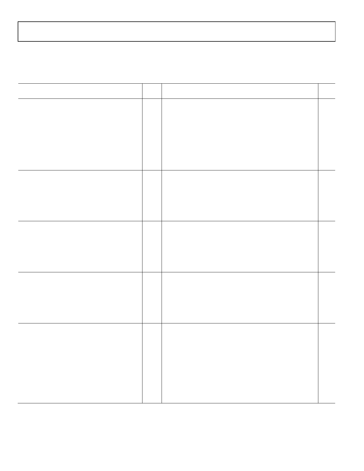
DIGITAL SPECIFICATIONS
AVDD = 1.8 V; DRVDD = 1.8 V, maximum sample rate, 2 V p-p differential input, 1.0 V internal reference; AIN = −1.0 dBFS,
DCS disabled, unless otherwise noted.
Table 3.
Parameter
DIFFERENTIAL CLOCK INPUTS (CLK+, CLK−)
Logic Compliance
Internal Common-Mode Bias
Differential Input Voltage
Input Voltage Range
High Level Input Current
Low Level Input Current
Input Resistance
Input Capacitance
LOGIC INPUTS (SCLK/DFS, SYNC, PDWN)1
High Level Input Voltage
Low Level Input Voltage
High Level Input Current
Low Level Input Current
Input Resistance
Input Capacitance
LOGIC INPUTS (CSB)2
High Level Input Voltage
Low Level Input Voltage
High Level Input Current
Low Level Input Current
Input Resistance
Input Capacitance
LOGIC INPUTS (SDIO/DCS)2
High Level Input Voltage
Low Level Input Voltage
High Level Input Current
Low Level Input Current
Input Resistance
Input Capacitance
DIGITAL OUTPUTS
DRVDD = 3.3 V
High Level Output Voltage, IOH = 50 μA
High Level Output Voltage, IOH = 0.5 mA
Low Level Output Voltage, IOL = 1.6 mA
Low Level Output Voltage, IOL = 50 μA
DRVDD = 1.8 V
High Level Output Voltage, IOH = 50 μA
High Level Output Voltage, IOH = 0.5 mA
Low Level Output Voltage, IOL = 1.6 mA
Low Level Output Voltage, IOL = 50 μA
AD9204-20/AD9204-40/AD9204-65/AD9204-80
Temp Min
Typ
Max
Full
Full 0.2
Full GND − 0.3
Full −10
Full −10
Full 8
Full
CMOS/LVDS/LVPECL
0.9
10
4
3.6
AVDD + 0.2
+10
+10
12
Full 1.2
Full 0
Full −50
Full −10
Full
30
Full
2
DRVDD + 0.3
0.8
−75
+10
Full 1.2
Full 0
Full −10
Full +40
Full
26
Full
2
DRVDD + 0.3
0.8
+10
+135
Full 1.2
Full 0
Full −10
Full +40
Full
26
Full
5
DRVDD + 0.3
0.8
+10
+130
Full 3.29
Full 3.25
Full
0.2
Full
0.05
Full 1.79
Full 1.75
Full
0.2
Full
0.05
1 Internal 30 kΩ pull-down.
2 Internal 30 kΩ pull-up.
Unit
V
V p-p
V
μA
μA
kΩ
pF
V
V
μA
μA
kΩ
pF
V
V
μA
μA
kΩ
pF
V
V
μA
μA
kΩ
pF
V
V
V
V
V
V
V
V
Rev. A | Page 6 of 36
Share Link: