ENW89815CXKF 查看數據表(PDF) - Panasonic Corporation
零件编号
产品描述 (功能)
生产厂家
ENW89815CXKF Datasheet PDF : 34 Pages
| |||
CLASSIFICATION
Einstufung
SUBJECT
Thema
CUSTOMER’S CODE
PAN1455/1555
PRODUCT SPECIFICATION
Produktspezifikation
CLASS 2 BLUETOOTH MODULE
Bluetooth Modul der Klasse 2
PANASONIC’S CODE
ENW89815CxKF/ENW89815AxKF
No.
REV.
DS-1x55-2400-102
1.10
PAGE
Seite
9 of 34
DATE
Datum
27.06.2011
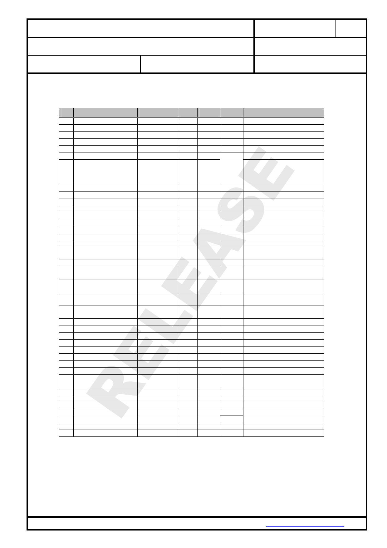
6.2.
APPLICATION SPECIFIC PIN DESCRIPTION
6.2.1. SPP configuration DCE Mode
No Pin Name
SPP-Function Type PU/PD Active Description
1 GND1
2 ANT
3 UART_RTS#
4 UART_TXD
5 UART_RXD
6 UART_CTS#
7 GPIO[9]/PCM_CLK
Power
Antenna
/RTS
TXD
RXD
/CTS
/LED2
P
-
-
I/O -
-
I
PU
L
I
PD
H
O
H
O
L
O
L
8 GPIO[10]/PCM_O/TXD3 UA2
9 GPIO[7]/PCM_SYNC
/LED1
10 GND2
Power
11 ATRST/SPI2_MISO
reserved
12 GPIO[8]/PCM_I/RXD3 /UE1
13 ATDI/SPI2_CS
reserved
14 ATMS
reserved
15 BOOT0
reserved
16 VCC
Power
17 RESET#
/RESET
O
O
L
-
-
-
I/O PU
H
I
PU
L
I/O PU
-
I
PU
-
I
PD
H
-
-
-
I
PU
L
18 GND3
19 GPIO[14]
Power
-
-
/RTC-OUT
O
L
20 GPIO[13]
/RTC-IN
I
PU
L
21 GPIO[15]
22 GPIO[6]/ADC
/DCD or /DCD- I/O PU
L
DTE
/RI
I/O PU
L
23 ATDO/SPI2_SCK
24 ATCK
25 GPIO[3]/SPI_CLK
26 GPIO[0]/SPI_MOSI
27 GND4
28 GPIO[2]/SPI_CS
29 GPIO[1]/SPI_MISO
30 GPIO[5]/TXD2
31 GPIO[4]/RXD2
32 USB_DM
33 USB_DP
34 GPIO[17]/TAMPER
A GPIO[16]/SPI2_MOSI
B GPIO[12]/I2C_SCL
C GPIO[11]/I2C_SDA
D VBAT
reserved
reserved
reserved
reserved
Power
reserved
/UE2
reserved
DTE-/DCE
Select
reserved
reserved
reserved
reserved
reserved
reserved
Power
O
PU
-
O
PD
-
I/O PD
H
I/O PD
H
-
-
O
I
PD
H
O
I
PD
H
I/O PD
-
I/O PD
-
I/O PD
-
I/O PU
L
I/O PU
L
I/O PU
L
-
-
Connect to Ground
Antenna Connector
UART Request To Send
UART Data Input
UART Data Output
UART Clear To Send
Bluetooth connected. Active if a
Bluetooth connection exists.
Inactive in idle state. Flashes
during startup.
User Output 2
Device Ready
Connect to Ground
leave open
User Input 1
leave open
leave open
for Debug-Use only, nc
VCC
Reset input (active low for 5 ms);
Schmitt triggered
Connect to Ground
DSR in DCE mode, DTR in DTE
mode
DTR in DCE mode, DSR in DTE
mode
Data Carrier Detect , Input in
DTE mode Output in DCE mode
Ring Indicator, Input in DTE
mode Output in DCE mode
JTAG
JTAG
leave open
leave open
Connect to Ground
leave open
User Input 2, Break Detect (1)
leave open
DTE (high) DCE (low) mode
selector
leave open
leave open
leave open
leave open
leave open
leave open
Optional Batterie Backup
Type: PU - Pulled up; PD – pulled down; P – Power; I – Input; O – Output; I/O - bidirectional
All other pins do not have a dedicated functionality in SPP mode. See 6.1 General Pin
Assignment for all other terminals.
PANASONIC ELECTRONIC DEVICES EUROPE GMBH
www.pedeu.pansonic.de
Share Link: 