FAN5601 查看數據表(PDF) - Fairchild Semiconductor
零件编号
产品描述 (功能)
生产厂家
FAN5601 Datasheet PDF : 15 Pages
| |||
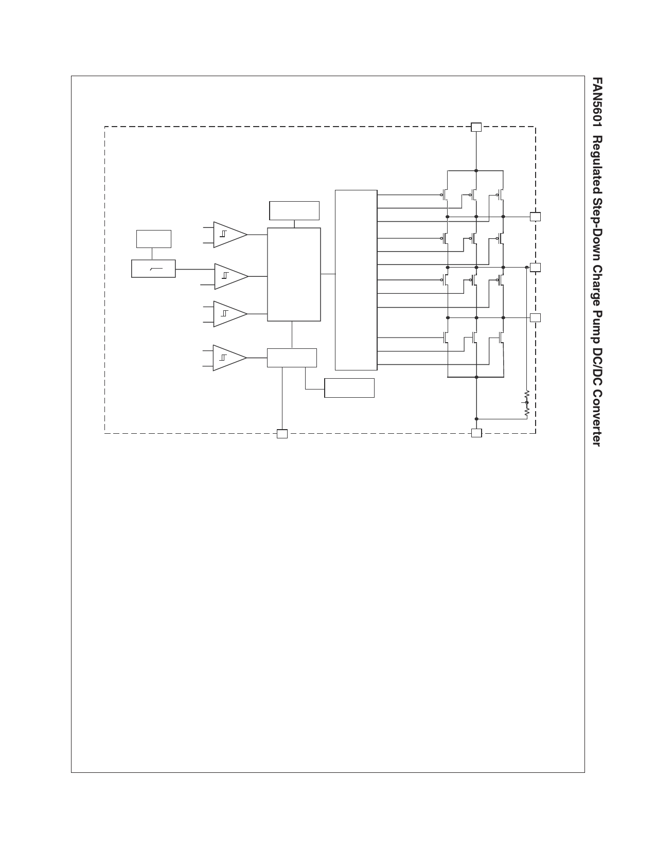
Block Diagram
V IN
VOLTAGE
REF.
OSCILLATOR
(2MHz)
IN - CONFIGURATION
OUT +
SOFT START
Vref RAMP
Vref RAMP - PULSE_SKIP
FB +
CONTROL
LOGIC
D
R
I
V
E
R
OUTPUT - SHORT_CKT.
S
150mV +
0.5* INPUT
-
1V +
UVLO
SHUTDOWN
THERMAL
SHUTDOWN
0.25SW1 0.25SW1 0.5SW1
C+
0.25SW2 0.25SW2 0.5SW2
0.25SW3 0.25SW3 0.5SW3
VOUT
C-
0.25SW4 0.25SW4 0.5SW4
FB
ENABLE
Detailed Description
The FAN5601 switched capacitor DC/DC converter automati-
cally configures switches to achieve a high efficiency and pro-
vides a regulated output voltage by means of pulse skipping,
pulse frequency modulation (PFM). An internal soft start circuit
prevents excessive inrush current drawn from the supply. Each
switch is split into three segments. Based on the values of VIN,
VOUT and IOUT, an internal circuitry determines the number of
segments to be used to reduce current spikes.
Step-Down Charge Pump Operation
When VIN ≥ 2.22 × VOUT, a 2:1 configuration shown in Fig.1(A)
is enabled. The factor 0.9 is used instead of 1 in order to
account for the effect of resistive losses across the switches and
to accommodate hysteresis in the voltage detector comparator.
Two phase non-overlapping clock signals are generated to drive
four switches. When switches 1 and 3 are ON, switches 2 and 4
are OFF and CB is charged. When switches 2 and 4 are ON,
switches 1 and 3 are OFF, charge is transferred from CB to
COUT.
When VIN <2.22 × VOUT, a 1:1 configuration shown in Fig. 1(B)
is enabled. In the 1:1 configuration switch 3 is always OFF and
the switch 4 is always ON. At 1.6V output setting the configura-
tion changes from 2:1 to 1:1 at VIN = 3.56V. At 1.3V output set-
ting the change occurs at VIN = 3.06V.
GND.
Pulse-skipping PFM and Fractional Switch
Operation
When the regulated output voltage reaches its upper limit, the
switches are turned off the output voltage reaches its lower limit.
Considering a step-down 2:1 mode of operation, 1.6V output as
an example, when the output reaches about 1.62V(upper limit),
the control logic turns off all switches. Switching stops com-
pletely. This is pulse-skipping mode. Since the supply is isolated
from the output, the output voltage will drop. Once the output is
dropped to about 1.58V(lower limit), the device will return to reg-
ular switching mode with one quarter of each switch turning on
first. Another quarter of each switch will be turned on if VOUT
cannot reach regulation by the time of arrival of the third charge
cycle. Full switch operation occurs only during startup or under
heavy load condition, when half switch operation cannot
achieve regulation within seven charge cycles.
Soft Start
The soft-start feature limits inrush current when the device is ini-
tially powered up and enabled. The reference voltage is used to
control the rate of the output voltage ramp-up to its final value.
Typical start-up time is 1ms. Since the rate of the output voltage
ramp-up is controlled by an internally generated slow ramp,
pulse-skipping occurs and inrush current is automatically lim-
ited.
10
www.fairchildsemi.com
FAN5601 Rev. 1.0.5
Share Link: 