LC709006A-TLM-E 查看數據表(PDF) - ON Semiconductor
零件编号
产品描述 (功能)
生产厂家
LC709006A-TLM-E Datasheet PDF : 14 Pages
| |||
LC709006A
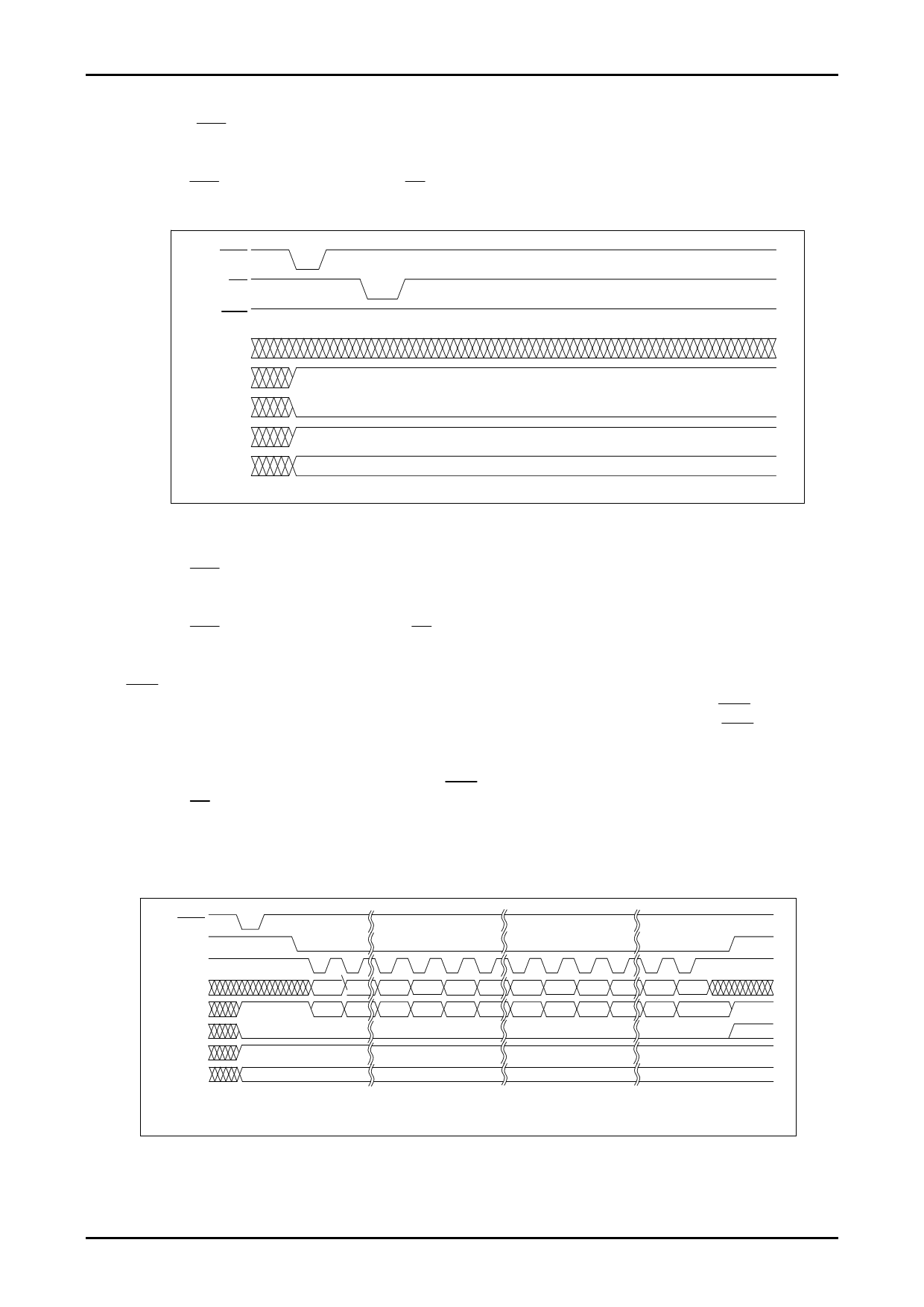
(1) Initial communication modes
• Mode 0
1) Setting the RES pin to the low level initializes the system, sets the DOUT pin to the high level, and sets the DDR
register of all ports to 0 and the DTR register to 1. The output type of the ports is set to Nch-open drain and their
I/O state (Nch-Tr=OFF) to the "Hi-Z" (input mode) state.
2) When the RES pin is set high (reset) and the CS pin is set and held low for a certain period (TwlCS), the DDR is
fixed at 0. Subsequently, the LC709006A is placed in the data communication mode.
RES
CS
CLK
DIN
DOUT
DDR
DTR
P00 to P27
Hi-Z
* DDR and DTR denote the state of the internal registers.
Fig. 1
• Mode 1
1) When the RES pin is set to the low level, the LC709006A initializes the system, sets the DOUT pin to the high
level, and sets the DDR register of all ports to 0 and the DTR register to 1. The output type of the ports is set to
Nch-open drain and their I/O state (Nch-Tr=OFF) to the "Hi-Z" (input mode) state.
2) When the RES pins is set high (reset) and the CS pin is set low, the LC709006A gets ready for serial
communication.
3) The input data at P00 is sent directly to the DOUT pin on the first falling edge of the transmission clock signal
CLK. The data at pins P01 to P27 is loaded into the shift register on the rising edge of the next clock.
4) Subsequently, the ports' input data, which is loaded into the shift register on the falling edge of CLK, is placed at
the DOUT pin sequentially (P00→P07, P20→P27) in synchronization with the falling edges of CLK, starting at
port pin P00. In parallel with this operation, when data to be placed at the ports is supplied to the DIN pin
sequentially starting at the port pin P00 (P00→P07, P10→P17, P20→P27), it is loaded into the internal shift
register in synchronization with the rising edges of CLK.
5) When the CS pin is set high after the rising edge of the 24th clock, the data loaded in the shift register is loaded
into the DDR register which determines the I/O mode and output type of the data (serial data is loaded into the
DDR register after a reset is effected). Subsequently, the LC709006A controls serial data transmission and
reception in the data communication mode.
RES
CS
CLK
DIN
DOUT
DDR
DTR
P00 to P27
0
1
6
7
8
9
14 15 16 17 22 23
P00_DR P01_DR P06_DR P07_DR P10_DR P11_DR P16_DR P17_DR P20_DR P21_DR P26_DR P27_DR
P00_DI P01_DI P06_DI P07_DI P10_DI P11_DI P16_DI P17_DI P20_DI P21_DI P26_DI
P27_DI
Hi-Z
Hi-Z
Hi-Z
Hi-Z
* PXX_DR denotes the input data to the port DDR identified by PXX.
* PXX_DI denotes the input data from the port pin identified by PXX.
Fig. 2
No.8265-9/14
Share Link: 