LC709004AMJ-AH 查看數據表(PDF) - ON Semiconductor
零件编号
产品描述 (功能)
生产厂家
LC709004AMJ-AH Datasheet PDF : 14 Pages
| |||
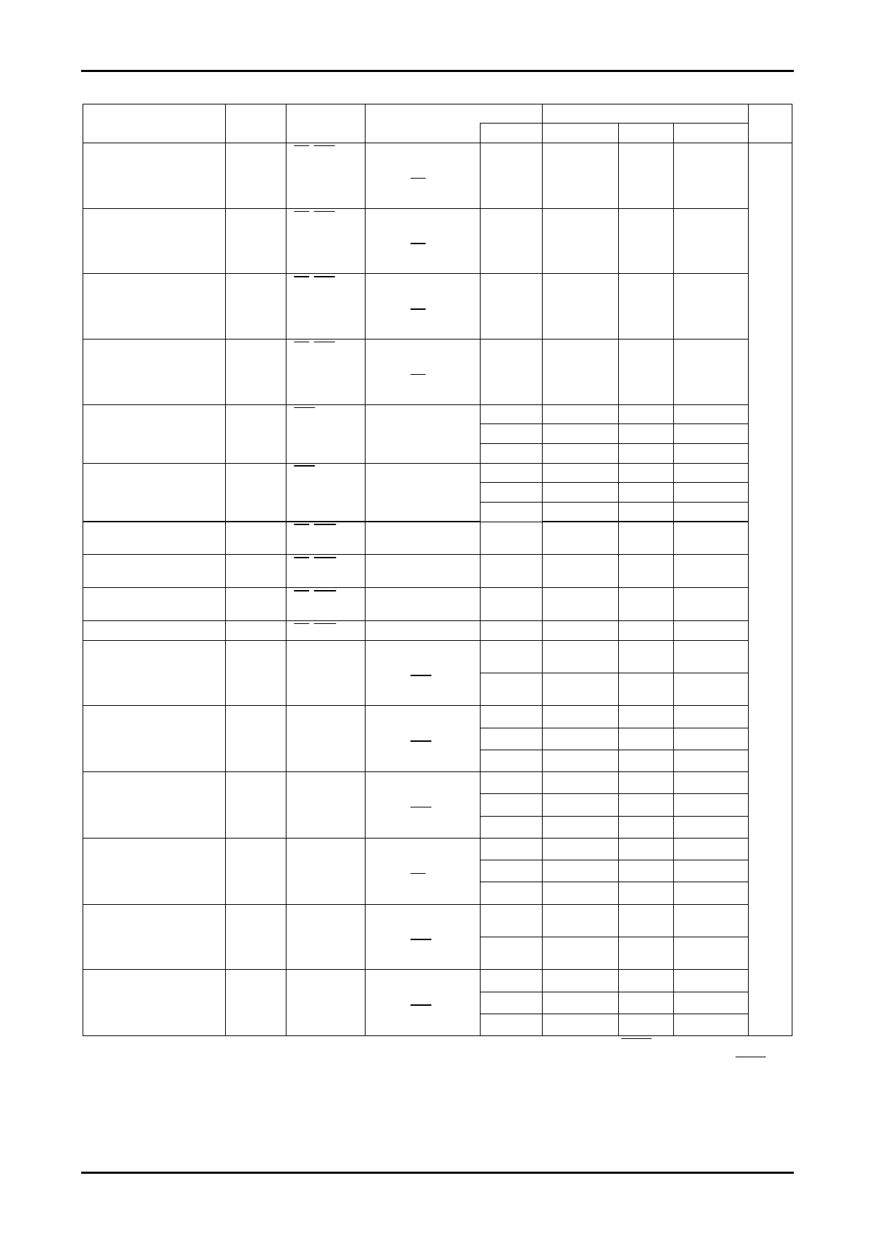
LC709004A
Switching I/O Characteristics at Ta=-30 to +70°C, VDD=VDDP1, VSS=0V
Parameter
Symbol Pin/Remarks
Conditions
VDD[V]
Specification (Note 3)
Unit
min
typ
max
Clock setup time
TsCLK
CS, CLK
•Specified with
respect to falling
2.0 to 6.0
100
edge of CS.
•See Fig. 8.
Chip select low level setup TslCS
CS, CLK
•Specified with
time
respect to falling
2.0 to 6.0
100
edge of CS.
•See Fig. 8.
Chip select low level hold ThlCS
CS, CLK
•Specified with
time
respect to falling
2.0 to 6.0
100
edge of CS.
•See Fig. 8.
Clock hold time
ThCLK
CS, CLK
•Specified with
respect to falling
2.0 to 6.0
200
edge of CS.
•See Fig. 8.
Clock low level pulse width TwlCLK CLK
•See Fig. 8.
4.5 to 6.0
250
2.7 to 6.0
500
2.0 to 6.0
1000
Clock high level pulse
TwhCLK CLK
•See Fig. 8.
4.5 to 6.0
250
width
2.7 to 6.0
500
2.0 to 6.0
1000
Chip select high level
TshCS
CS, RES
•See Fig. 8.
2.0 to 6.0
200
setup time
Chip select high level hold ThhCS
CS, RES
•See Fig. 8.
2.0 to 6.0
100
time
Chip select low level pulse TwlCS
CS, RES
•See Fig. 8.
ns
2.0 to 6.0
200
width
Reset low level pulse width TwlRES CS, RES
•See Fig. 8.
2.0 to 6.0
150
Data setup time
Data hold time
TsDIN
DIN
•Specified with
4.5 to 6.0
30
respect to falling
edge of CLK.
2.0 to 6.0
50
•See Fig. 8.
ThDIN
DIN
•Specified with
4.5 to 6.0
50
respect to falling
edge of CLK.
2.7 to 6.0
150
•See Fig. 8.
2.0 to 6.0
300
Serial data output delay
TdD0UT DOUT
•Specified with
4.5 to 6.0
200
time
(Note 4)
respect to falling
2.7 to 6.0
400
edge of CLK.
•See Fig. 8.
2.0 to 6.0
800
Port data output delay time TdPOUT Port 0 to 1
•Specified with
4.5 to 6.0
200
respect to rising
edge of CS.
2.7 to 6.0
400
•See Fig. 8.
2.0 to 6.0
800
Port data input setup time TsPIN
Port 0 to 1
•Specified with
4.5 to 6.0
30
respect to rising
edge of CLK.
2.0 to 6.0
50
•See Fig. 8.
Port data input hold time
ThPIN
Port 0 to 1
•Specified with
4.5 to 6.0
50
respect to rising
2.7 to 6.0
150
edge of CLK.
•See Fig. 8.
2.0 to 6.0
300
Note 4: The input data of P00 will be out from DOUT terminal at the first negative edge of CLK signal. Because of this,
Serial data output delay time of the first clock will be the time measured from the negative edge of the CLK or
the time at the input data (P00) is settled.
No.A0165-4/13
Share Link: 