CXB1567Q 查看數據表(PDF) - Sony Semiconductor
零件编号
产品描述 (功能)
生产厂家
CXB1567Q Datasheet PDF : 16 Pages
| |||
CXB1567Q
Notes on Operation
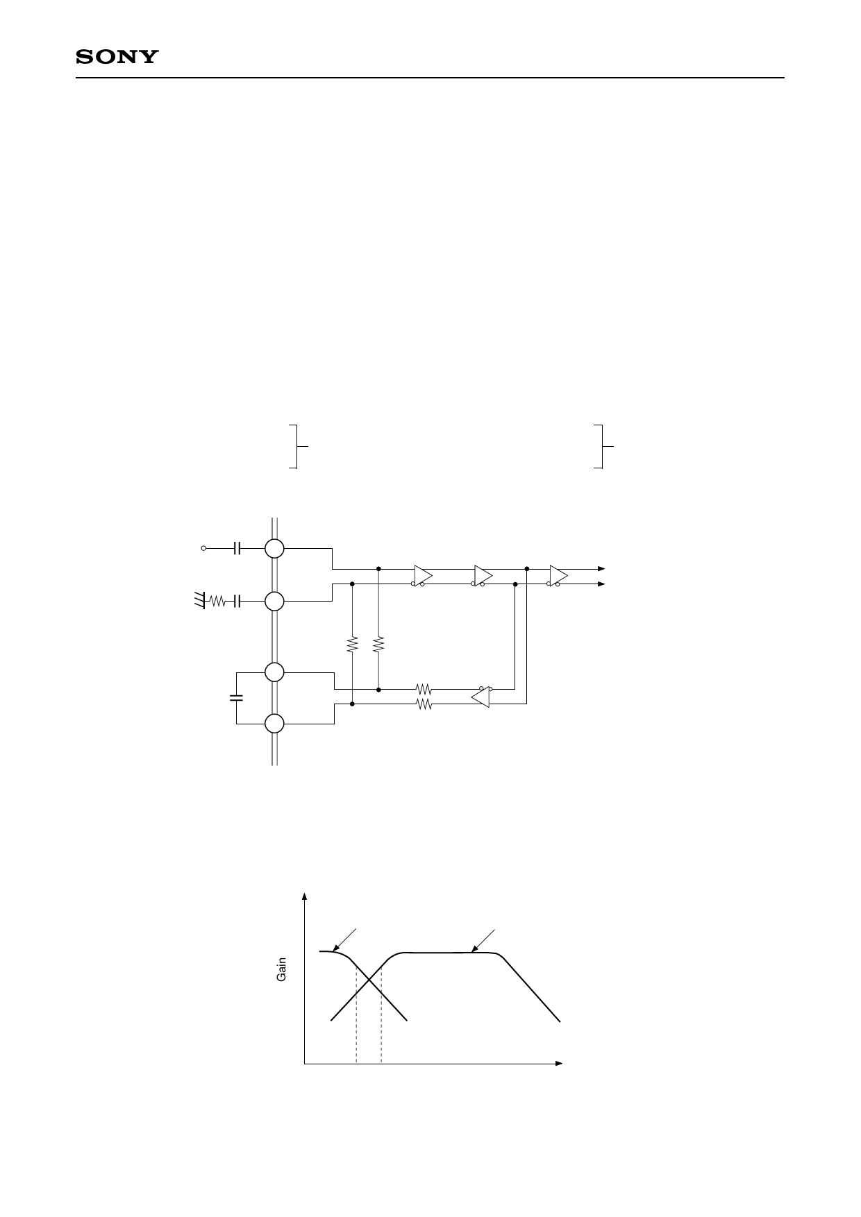
1. Limiting amplifier block
The limiting amplifier block is equipped with the auto-offset canceller circuit. When external capacitors C1 and
C2 are connected as shown in Fig. 1, the DC bias is set automatically in this block. External capacitor C1 and
IC internal resistor R1 determine the low input cut-off frequency f2, as shown in Fig. 2. Similarly, external
capacitor C2 and internal resistor R2 determine the high cut-off frequency f1 for DC bias feedback. Since
peaking characteristics may occur in the low frequency area of the amplifier gain characteristics depending on
the f1/f2 combination, set the C1 and C2 values so as to avoid the occurrence of peaking characteristics. The
typical values of R1,R2, C1 and C2 are as indicated below. When a single-ended input is used, provide AC
grounding by connecting Pin 10 to a capacitor which has the same capacitance as capacitor C1. RD is the
resistor for impedance matching. The same level of output impedance as for the signal source should be
applied to Pin 10.
R1 (internal) : 1kΩ
C1 (external) : 1000pF
f2: 160kHz
R2 (internal) : 7.5kΩ
C2 (external) : 0.047µF
f1: 450Hz
D
8
C1
RD
10
C1
15
C2
16
R1
R1
R2
R2
Fig. 1
To IC interior
Feedback frequency
responce
Amplifier frequency
responce
f1 f2
Frequency
Fig. 2
– 10 –
Share Link: 