TRCV012G5 查看數據表(PDF) - Agere -> LSI Corporation
零件编号
产品描述 (功能)
生产厂家
TRCV012G5
Agere -> LSI Corporation

TRCV012G5 Datasheet PDF : 28 Pages
| |||
Preliminary Data Sheet
August 2000
TRCV012G5 and TRCV012G7
Limiting Amplifier, Clock Recovery, 1:16 Data Demultiplexer
Clock and Data Recovery (CDR)
Clock Recovery Operation
The CDR circuit uses a PLL to extract the clock and retime the 2.5 Gbits/s data. The 2.5 Gbits/s data and the
2.5 GHz recovered clock are available as outputs, as well as a 155 MHz clock derived from the recovered clock.
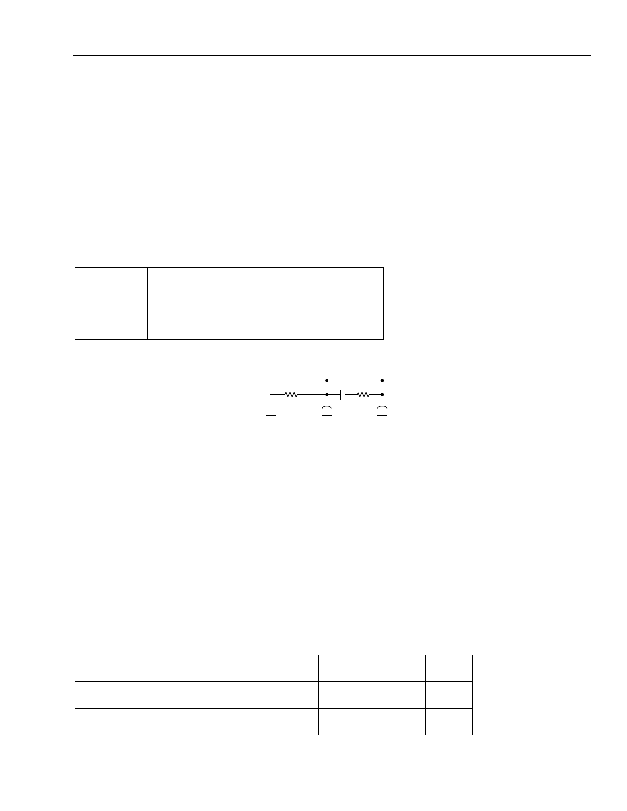
Clock Recovery PLL Loop Filter
A typical loop filter that meets the OC-48 jitter transfer template is shown in Figure 4. Connect the filter compo-
nents and also connect LFP to VCP and connect LFN to VCN. The component values can be varied to adjust the
loop dynamic response (see Table 5).
Table 5. Clock Recovery Loop Filter Component Values
Components
C1*
C2, C3
R1
R2
Values for 2 MHz Loop Bandwidth
0.47 µF ± 10%
10 pF ± 20%
82.5 Ω ± 5%
100 kΩ ± 5%
* Capacitor C1 should be either ceramic or nonpolar.
LFP/VCP LFN/VCN
R2
C1 R1
C2
C3
Figure 4. Clock Recovery PLL Loop Filter Components
5-8061(F).a
CDR Acquisition Time
The limiting amplifier plus CDR will acquire phase/frequency lock within 10 ms after powerup and a valid SONET
signal or a 223 – 1 PRBS data signal is applied.
CDR Generated Jitter
The limiting amplifier plus CDR’s generated jitter performance meets the requirements shown in Table 6. These
specifications apply to the jitter generated at the 2.5 Gbits/s recovered clock pins (CK2G5P/N) when the following
occur: no jitter is present on the input, the limiting amplifier’s input signal is within the valid level range given in
Table 9 on page 20, and the data sequence is a valid OC-48 SONET/SDH signal.
Table 6. Clock and Data Recovery Generated Jitter Specifications
Parameter
Generated Jitter (p-p):
Measured with 12 kHz to 20 MHz Bandpass Filter
Generated Jitter (rms):
Measured with 12 kHz to 20 MHz Bandpass Filter
Typical
0.06
0.008
Max
(Device)*
0.10
0.01
Unit
UIp-p
UIrms
* This denotes the device specification for system SONET/SDH compliance when the loop filter in Table 5 and Figure 4 is used.
Lucent Technologies Inc.
11
Share Link: