TRCV012G5 查看數據表(PDF) - Agere -> LSI Corporation
零件编号
产品描述 (功能)
生产厂家
TRCV012G5
Agere -> LSI Corporation

TRCV012G5 Datasheet PDF : 28 Pages
| |||
Preliminary Data Sheet
August 2000
TRCV012G5 and TRCV012G7
Limiting Amplifier, Clock Recovery, 1:16 Data Demultiplexer
Pin Information (continued)
Note: In Table 1, when operating the TRCV012G7 device at the OC-48/STM-16 rate, 2.5 Gbits/s should be inter-
preted as 2.48832 Gbits/s. When operating the TRCV012G7 device at the RS FEC OC-48/STM-16 rate,
2.5 Gbits/s should be interpreted as 2.66606 Gbits/s. (A similar interpretation should be made for 2.5 GHz.)
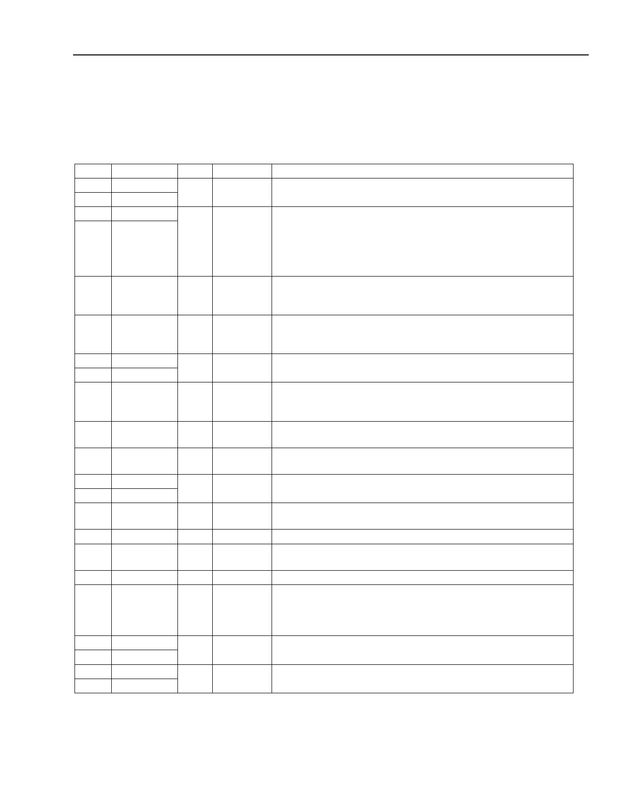
Table 1. Pin Descriptions—2.5 Gbits/s and Related Signals
Pin Symbol* Type† Level
Name/Description
30
LAINP
32
LAINN
I
Analog Limiting Amplifier Inputs (2.5 Gbits/s).
ac coupling required.
50
D2G5P
O
51
D2G5N
CML
Data Output (2.5 Gbits/s NRZ). 2.5 Gbits/s differential data
output.
s Pins are high impedance when END2G5N = 1.
s Pins are active but forced to differential logic low when
MUTE2G5N = 0.
122 END2G5N Iu
118 MUTE2G5N Iu
CMOS
CMOS
Enable D2G5P/N Data Outputs (Active-Low).
0 = D2G5P/N buffer enabled
1 or no connection = D2G5P/N buffer powered off
Mute D2G5P/N Data Output (Active-Low).
0 = muted
1 or no connection = normal data
53
CK2G5P
O
54 CK2G5N
123 ENCK2G5N Iu
CML
CMOS
Recovered Clock Output (2.5 GHz). 2.5 GHz recovered differen-
tial clock output. Pins are high impedance when ENCK2G5N = 1.
Enable CK2G5P/N Clock Output (Active-Low).
0 = CK2G5P/N buffer enabled
1 or no connection = CK2G5P/N buffer powered off
41
RREF1
I
Analog Resistor Reference 1. CML current bias reference resistor. (See
Table 16, page 22 for values.)
40
RREF2
I
Analog Resistor Reference 2. CML bias reference resistor. Place a
1.5 kΩ resistor to VCCD.
28
VTHP
34
VTHN
I
Analog Voltage Threshold Adjust Input. This input is for monitoring
purposes only and should be left open (see Figure 3 on page 10).
26
SLADJ
I
Analog Slice Level Adjustment. Adjusts slice level for the limiting amp
(see Figure 3 on page 10).
119 LOSAN
O Open Drain Loss of Analog Signal (Active-Low).
25 PRG_LOSA I
Analog Programming Voltage for LOSA Threshold. Programming
voltage is scaled (see Figure 7 on page 16).
120 LOSDN
121 INLOSN
O Open Drain Loss of Digital Data (Active-Low).
Iu
CMOS Input Loss of Signal (Active-Low). Forces VCO to decrease to
its minimum frequency.
0 = force VCO low
1 or no connection = normal operation
18
LFP
O
Analog Loop Filter PLL. Connect LFP to VCP, and LFN to VCN.
17
LFN
19
VCP
I
Analog VCO Control. Connect VCP to LFP, and VCN to LFN.
16
VCN
* Differential pins are indicated by the P and N suffixes. For nondifferential pins, N at the end of the symbol name designates active-low.
† I = input, O = output. Iu = an internal pull-up resistor on this pin, Id = an internal pull-down resistor on this pin, It = an internal termination
resistance of 50 Ω on this pin.
Lucent Technologies Inc.
5
Share Link: